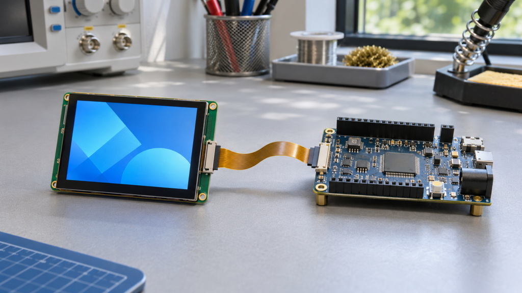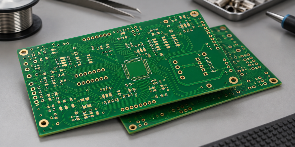
Double layer PCB manufacturing turns a copper-clad insulating core into a board with conductive patterns on both faces. In a common plated-through-hole process, the fabricator drills the panel, makes selected hole walls conductive, images the circuit, plates and etches copper, applies solder mask and surface finish, then profiles and tests the bare boards.
A two-layer board is not automatically suitable for every display controller. Its copper geometry, return-current paths, power, connectors, manufacturing tolerances and test requirements must fit the actual design. This guide follows a representative rigid-board process and explains what an OEM or electronics engineer should establish before ordering.
What is a double layer PCB?
A double layer or double-sided PCB has two patterned copper conductor layers, normally one on each face of an insulating core. The solder mask and printed legend are additional materials but are not counted as copper circuit layers. FR-4 is one common family of rigid laminate; the exact grade and finished construction should be specified for the application.
Conductors on opposite sides can be connected by plated-through holes (PTHs), including vias and component holes, when the design calls for them. A double-sided board can also contain non-plated holes for mounting or other purposes. Having two copper faces does not mean every hole is plated or every overlapping pad is electrically connected.[1]
A bare PCB provides the physical interconnections. A printed circuit board assembly (PCBA) is the board after components have been mounted and soldered. Fabrication, assembly and functional testing have related but distinct data and acceptance requirements.
How is a two-layer PCB manufactured?
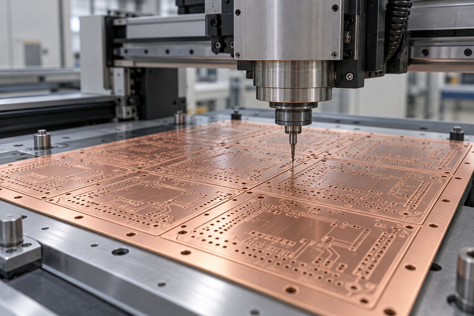
The sequence below is a representative pattern-plated, subtractive process for a rigid PTH board. A fabricator can use another sequence, chemistry or imaging method. Confirm the actual process and capability with the selected supplier; the flow is not a claim about RJY’s own factory processes.[2][3]
| Etapa | Propósito | Critical output |
|---|---|---|
| Revisión de ingeniería | Check the design package and manufacturing notes. | Resolved data, layer mapping and agreed requirements. |
| Material preparation | Cut a double-sided copper-clad laminate into production panels. | Correct core, copper and workable panel size. |
| Drilling and hole preparation | Create holes and prepare the hole walls. | Correct locations and clean surfaces for subsequent processing. |
| Hole metallization and plating | Create conductive paths through specified holes. | A continuous plated connection where required. |
| Imaging, plating and etching | Define and form the copper circuit. | Traces, pads and isolated areas that match the design. |
| Mask, finish and legend | Protect selected copper, prepare exposed pads and add markings. | Openings, finish and markings consistent with the files. |
| Profile and final inspection | Separate boards and check the finished product. | Required outline, electrical results and inspection records. |
1. Review the fabrication package
The fabricator starts with the circuit images, drill data, board outline and fabrication drawing. The engineer checks that the files use the same origin, units and revision, and that the top and bottom copper layers align with the plated and non-plated hole information. A netlist provides a useful independent electrical reference.
Manufacturing review also addresses material, finished thickness, copper requirements, minimum features, hole tolerances, surface finish, solder-mask openings and board profile. A missing note can become a supplier assumption. Resolve conflicting requirements before a production panel is made.
2. Cut and prepare the copper-clad core
A common rigid starting material is an insulating core clad with copper on both sides. The supplier cuts it into a panel suitable for its process and cleans the surfaces. The initial copper foil is not necessarily the same as the finished copper thickness: subsequent plating and processing can change the copper in the finished features.
Do not specify only “two-layer FR-4” if the application has specific thermal, dielectric, mechanical or assembly constraints. Identify the relevant laminate grade, thickness and copper requirements with tolerances appropriate to the design. A fabricator should confirm what it can produce and inspect.
3. Drill holes and prepare the walls
Mechanical drilling creates the holes indicated in the drill data. Production panels use registration and tooling features so holes and artwork can be aligned. After drilling, the shop cleans and prepares the holes for the selected metallization process. The treatment and its sequence depend on the material and the manufacturer’s process.
Finished hole size is not always the same as drill size. For a plated hole, the plating reduces the final opening; the fabricator selects the drill and process compensation to meet the agreed finished-hole tolerance. Clearly identify which holes are plated, which are non-plated, and which dimensions are finished dimensions.
4. Make plated holes conductive
The insulating hole wall cannot carry current on its own. A common method deposits a thin conductive copper layer chemically, after which electrolytic copper can build up the conductor and plated hole. Alternative direct-metallization methods also exist. The exact sequence of panel plating, imaging and pattern plating varies by shop.[2][4]
Continuity between the two sides depends on a sound hole-wall connection and contact to the intended pads. Hole size, board thickness, pad geometry, material and process capability all matter. Electrical continuity is useful evidence, but it does not by itself prove every long-term reliability requirement.
5. Image, plate and etch the copper pattern
In the representative pattern-plating route, photoresist is applied and exposed to define where copper and an etch-resistant metal will be plated. After development and plating, the resist is removed. Etching removes unwanted exposed copper; the remaining protective metal is then stripped or handled according to the selected finish route. Georgia Tech’s process description shows this example sequence.[2]
Other processes use different imaging and plating sequences. The result required by the design remains the same: conductive features where the netlist requires them and isolation where circuits must remain separate. Review trace width, spacing, annular ring and hole-to-copper clearance against the fabricator’s current capabilities.
6. Apply solder mask, surface finish and markings
Solder mask covers selected areas of copper and leaves intended openings for pads and other features. It can help control solder bridging during assembly, but it is not a substitute for a specified electrical insulation system. Mask registration and the size of mask openings matter around fine-pitch components.
A surface finish protects exposed copper and supports the intended soldering or contact function. Options can include lead-free HASL, ENIG, OSP or other finishes, subject to the fabricator’s capabilities and project needs. Compare solderability, surface flatness, storage and assembly requirements rather than assuming one finish is best for every design.
Legend or silkscreen identifies items such as reference designators and polarity marks. It is not part of the circuit connectivity. Avoid placing markings where they interfere with exposed solder pads or create ambiguity at inspection.
7. Profile, test and inspect
The manufacturer forms the outline by routing, scoring or another agreed method. Panelization features and breakaway tabs must be compatible with assembly and depanelization. The board is then inspected against the agreed drawing and acceptance requirements. A bare-board electrical test checks for specified opens and shorts; the chosen method and coverage depend on the design and test arrangement.
Visual or automated optical inspection can identify certain defects in copper patterns or finished surfaces. Cross-sectioning and other destructive or sample-based checks can provide evidence about internal features such as plated-hole construction when required by the agreed plan. Neither visual inspection nor a continuity pass alone proves that the assembled controller will operate correctly.
Double layer PCB manufacturing versus PCB assembly
| Work | Main input | Output or check |
|---|---|---|
| Bare-board fabrication | Copper layers, drill files, outline, netlist and fabrication notes. | Unpopulated PCB with specified conductor pattern and finish. |
| Assembly | Bare board, bill of materials, placement data, polarity and assembly instructions. | Components mounted and soldered to create a PCBA. |
| Functional validation | Test procedure, firmware, fixtures and acceptance limits. | Evidence that the specified assembly performs its intended functions. |
Do not assume that a bare-board order includes parts, programming or a display test. For a display controller assembly, distinguish a bare-board electrical test from checking power rails, video output, backlight behavior, touch and software on the assembled system.
What files are needed to manufacture a double-sided PCB?
A complete release package reduces avoidable questions. The exact format depends on the fabricator, but the following information is normally useful:
- Copper artwork: top and bottom layer data, with an unambiguous view convention and common origin.
- Mask and legend: top and bottom files and any required opening or marking notes.
- Drill data: locations, tool definitions, units and separate plated and non-plated identification.
- Outline and fabrication drawing: dimensions, thickness, tolerances, cutouts and panel requirements.
- Electrical netlist: the expected connectivity for comparison and test where supported.
- Fabrication notes: material, copper, hole requirements, surface finish, applicable acceptance criteria and documentation.
For assembly, add the controlled BOM, placement or centroid data, assembly drawing, polarity and orientation information, and any programming or test instructions. Specify revisions for the board and assembly separately. A Gerber set alone does not necessarily communicate every construction or acceptance requirement.
Design-for-manufacturing decisions that affect yield and cost
Trace width, spacing and copper
Trace width and spacing must meet both electrical needs and the fabricator’s capability for the specified copper and process. Fine features can require tighter process control and raise cost or reduce the available supplier pool. Copper thickness affects current-carrying and thermal behavior, but a width or copper weight alone does not guarantee a temperature rise or current rating. Use an appropriate calculation method and validate the completed design.
Vias, annular rings and finished holes
Allow for drill registration and the fabricator’s required annular ring. Very small holes, thick boards and dense pad fields can constrain drilling and plating. Specify a finished-hole tolerance where a component or connector must fit, and confirm the supplier’s tooling and inspection plan. A through via connects the two copper faces only when the plated path and pads are correctly defined and manufactured.
Board outline, clearances and panelization
Keep copper, components and mounting features clear of the board edge according to the design and supplier’s process. Define the finished outline, cutouts and keepouts. If the board will be assembled in a panel, agree on rails, fiducials, tabs or scoring with both the assembler and fabricator. The final decision must also protect connectors and nearby components during depanelization.
Surface finish and assembly
Fine-pitch parts, storage duration, multiple soldering operations and connector contacts can influence finish selection. Confirm the applicable finish, handling and assembly constraints with the supplier. A finish name alone does not establish solderability after an unspecified storage period or guarantee a reliable connector interface.
When is a two-layer PCB a good choice?
Two copper layers can be a practical starting point for a relatively simple circuit when routing, grounding, power and manufacturing requirements can all be met. They offer space on both sides of the core and allow connections between faces through suitable vias. They are not inherently the least expensive or most reliable choice for every product; the full design and production volume affect the trade-off.
A four-layer or other multilayer board can provide additional routing and reference-plane options. For higher-speed interfaces, dense connectors or multiple power domains, a two-layer layout may be more difficult to implement with a continuous return path and the required impedance. The layer count alone does not prove signal integrity: review the stackup, geometry, return currents, connector transitions and actual interface requirements.
What changes for an LCD controller or HMI board?
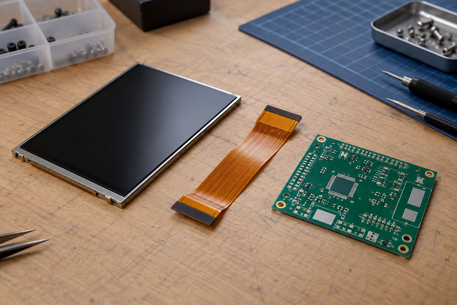
A display-related PCBA may connect a host, LCD module, backlight and touch controller. The board’s job can range from simple power or control circuitry to a complex interface or processor-based design. Confirm the system architecture before deciding the copper-layer count.
For any controller-board match, review the actual LCD model, resolution, interface, pin definition, timing, driver IC where available, power rails, backlight and touch requirements. Firmware, operating system and the mechanical environment are also project-dependent. Similar connectors do not guarantee electrical compatibility, and HDMI-to-MIPI conversion is not a universal passive cable.
High-speed links such as LVDS, MIPI, HDMI or eDP may need carefully controlled impedance and return paths. Consult the relevant interface and component documentation and work with the PCB fabricator on the stackup. Do not assume that every two-layer board can meet these requirements or that every design requires the same number of layers.
For related terminology, see what a PCB board is made of; that guide covers materials and structures, while this article focuses on manufacturing and release decisions.
How to set inspection and acceptance requirements
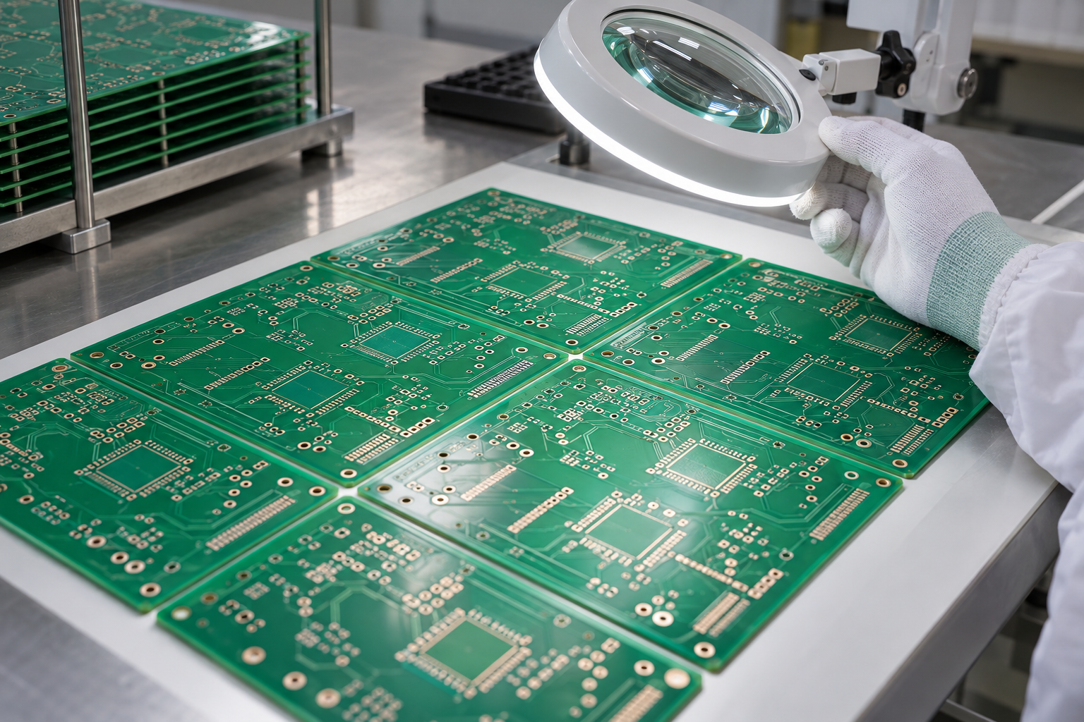
Agree on the applicable standard, revision, product class or equivalent acceptance criteria in the purchase documents. Do not use a standard’s name as proof that a supplier or specific board is certified. Ask what evidence will be provided for the order, such as material identification, electrical-test results, dimensional inspection, sample cross-sections or traceability, where required.
Describe the critical features: connector holes, finished thickness, edge clearance, plated-hole quality, solder-mask openings and relevant finish. For an assembled board, add assembly inspection, programming and functional test requirements. A prototype should be evaluated with its actual connector, enclosure, power and display rather than only against a catalog description.
Common questions about double layer PCB manufacturing
Is a double-sided PCB the same as a two-layer PCB?
In this context, both terms describe a board with patterned copper on two faces. Clarify whether the required interconnections are plated and how the layers are defined in the order.
Are all holes in a two-layer PCB plated?
No. A design can include plated holes for electrical connections and non-plated holes for mechanical features. Identify each type clearly in the drill data and drawing.
Can a two-layer PCB carry high-speed display signals?
It can be evaluated for a particular interface and layout, but two layers do not guarantee acceptable impedance, return paths or signal integrity. Review the complete stackup, routing and system requirements.
Does passing a bare-board electrical test prove the PCBA works?
No. Bare-board testing checks the specified electrical connectivity and isolation. Component assembly, firmware, power and system behavior require their own checks.
Is solder-mask color a measure of PCB quality?
No. Color alone does not establish material properties, registration, electrical behavior or manufacturing quality. Evaluate the specified material and inspection results.
What should I send for a manufacturing quote?
Provide the board files, drill data, outline, netlist and fabrication drawing with material, copper, finish, tolerances, quantity and inspection requirements. Add BOM and assembly data if an assembled board is needed.
Discuss a display-board project
Two-layer fabrication is a sequence of material preparation, hole formation, metallization, copper patterning, protection and verification. The useful purchasing question is whether the specified process can produce and verify the board your design requires.
For an LCD module or controller-board integration project, share the panel model and datasheet, host interface, power and backlight needs, touch requirements, board files and intended operating environment. Contacte con RJY Display for a project-specific discussion.
Referencias
- Defense Logistics Agency, MIL-PRF-31032/2 document details, scope for rigid single- and double-layer printed boards with or without plated holes.
- Georgia Tech, PWB Fabrication Process.
- PCBWay, PCB Manufacturing Process, example double-sided flow.
- Unimicron Germany, Plating Through and Photo Print.