FMMレスOLEDパターニングは、製造業者がディスプレイ全体に赤、緑、青の発光領域をどのように配置するかを変える。その目的は、関連するパターニング工程においてファインメタルマスクへの依存を低減しつつ、有用な画素構造を形成することにある。工学的課題は、OLED材料と意図した幾何学的形状の両方を維持することである。.
公開開示は、その目標に向けた複数の経路を記述している。それらは堆積、保護、選択的パターン形成、および封止において異なる。それらの違いを理解することは、「マスクレス」を単一の製造レシピとして扱うよりも重要である。本分析は、2026年10月20日時点で利用可能な公開証拠を検討し、その後、スケールアップを決定づけるプロセス上の課題を説明する。.
ファインメタルマスクは堆積材料をサブピクセル位置に配置する
ファインメタルマスク(FMM)は、小さな開口部を有する薄い金属板である。Samsung Displayが記述した堆積アプローチでは、それらの開口部が蒸発した有機材料を意図したサブピクセル位置へ導く。色ごとに異なるマスクが、赤、緑、青の順次堆積を支える。.[1]
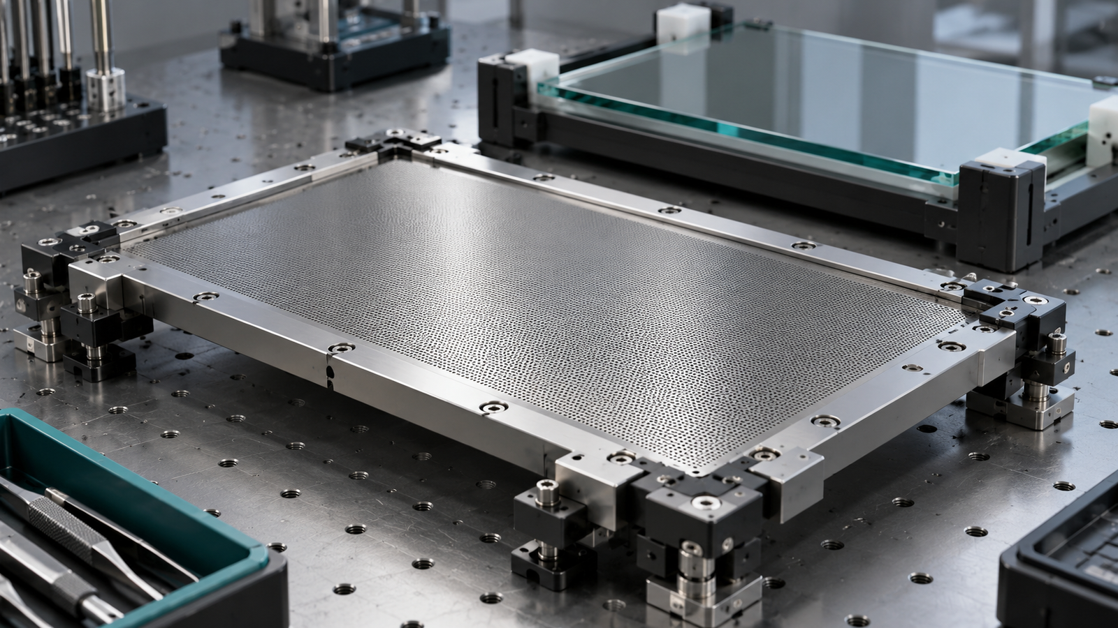
したがってマスクは、材料堆積プロセス内で幾何学的な役割を果たす。その開口部、位置、および基板との関係が、材料が到達する場所に影響を与える。プロセスは、パターニングされる領域全体にわたってその関係を維持しなければならない。.
より大きなマスクは撓みや反りが生じ、基板との位置合わせが変化し得る。.[3] マスクと基板の間のギャップも、開口部においてシャドウ領域を生じさせ、微細フィーチャの忠実度に影響を与え得る。.[6] 結果として生じる限界は、プロセスと設備に依存する。.
また、微細パターニングと広面積コーティングを区別することも有用である。Samsung Displayは、より大きなディスプレイ領域や共通層への堆積用のオープンマスクについて別途記述している。.[2] 直接RGBアプローチは色形成経路の一つであり、すべてのOLEDプロセスの記述ではない。特定の工程からFMMを除去しても、工場からすべてのマスク、治具、またはリソグラフィ工程が除去されるわけではない。.
FMMレス経路はパターニング課題を他のプロセス工程に移転する
有用な問いは、FMMの幾何学的機能を何が代替するかである。プロセスは依然として、発光材料が残る場所、別の色が形成できる場所、および隣接領域がどのように区別されるかを選択する必要がある。また、既に配置された材料を保護しなければならない。.
LG Displayは、2026年8月のIMIDにおいて、FMMレス革新的画素パターニング技術であるFLiPPを発表した。その公開記述は、堆積またはコーティングと、保護、パターン除去、およびフォトリソグラフィを組み合わせている。同社はまた、その実装において第8.5世代マザーガラス全体の処理を報告した。.[3]
2026年10月11日の韓国語によるLG Displayの報告は、10月8日のセミナーを記述した。それは、堆積、封止または保護膜、およびUV関連の除去工程を伴うフォトパターニングを含む、連続的なRGB処理の概要を示した。.[4] これは公開されたプロセスの概要であり、それを再現するために必要な完全な条件ではない。.
中心的なトレードオフは場所を変える。プロセスはファインメタルマスクへの依存を低減しつつ、選択的パターン形成、保護、および除去の重要性を高め得る。全体的な結果は、単に一つのツールの不在ではなく、それらの操作がどのように連携するかに依存する。.
公開経路をその明示されたプロセス機能によって比較する
Applied Materialsは2024年11月にMAX OLEDを発表した。その記述は、特許取得済みの画素アーキテクチャと、マスクレス選択堆積および個別画素封止を組み合わせている。それは堆積、封止、および材料ハンドリングを統合された設備アプローチとして提示している。リリースは、Appliedが技術を評価するためにSamsung Displayにアルファシステムを供給すると述べた。.[5]
その日付は発表された評価計画を確立するものである。それはシステムの現在の展開段階を確立するものではない。同様に、設備プラットフォームと認定済み完成パネルは、異なる製品であり異なる証拠を表す。.
| 公開経路 | 開示における重点 | 有用な解釈 |
|---|---|---|
| LG Display FLiPP | 保護された有機層処理とフォトパターニング | 選択的形成と材料保護が連続する色間でどのように機能するかを検討する。. |
| Applied Materials MAX OLED | 選択堆積、画素アーキテクチャ、および個別画素封止 | 統合プロセスと意図されたパネル用途に関する証拠を検討する。. |
| 学術的間接フォトパターニング | 直接処理損傷を限定しつつ発光パターンを形成する実験室的方法 | 材料制約とデバイス検証を理解するために用いる。. |
比較は公開アプローチを記述するものであり、それらを順位付けしたり、共通の知的財産を確立したりするものではない。また、FMMレスが定義上インクジェット印刷を特定するものでもない。この用語は変化したプロセス依存性を特定するものであり、代替方法にはそれ自体の記述が必要である。.
パターン忠実度は有機デバイスが依然として機能する場合にのみ重要である
きれいに見えるパターンは中間結果である。パターニングされた有機材料は、完成デバイスに必要な電気的および光学的挙動を保持しなければならない。材料を光、化学薬品、または除去工程に曝露するプロセスは、したがって幾何学的検査以上のものを必要とする。.
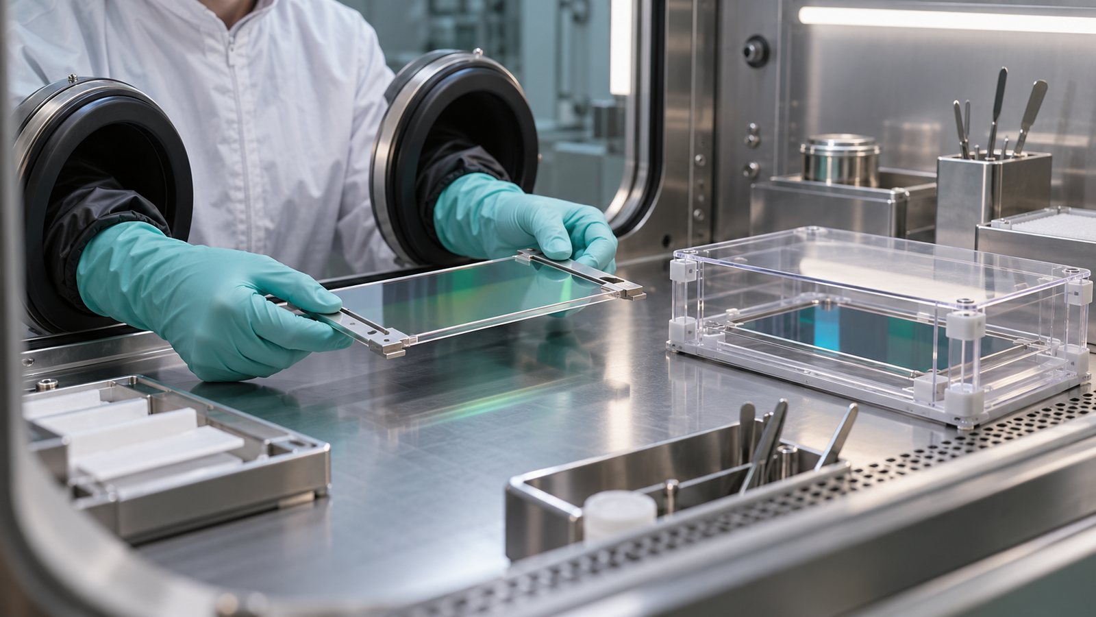
2025年7月のLight: Science & Applications誌の論文は、溶液処理されたRGB発光層の間接フォトパターニングを実証した。研究は、犠牲フォトレジストとネットワーク形成を用いて、損傷を与える処理条件への直接曝露を低減した。それは、有機発光材料のUV、溶媒、およびエッチングに対する感受性に対処するものである。.[6]
この研究は実験室実証である。それは材料保護がなぜ中核的な工学的課題であるかを説明するのに役立つが、LG DisplayやApplied Materialsが使用する専有プロセスを特定するものではない。.
我々の提案する評価は、パターニング後のデバイスから始まる。その電気的挙動、光出力、色、および経時変化を適切な参照と比較する。次に、パターン境界、均一性、および隣接色の処理の影響を評価する。成功した形状と成功したOLEDデバイスは関連する結果であり、別々の証拠を必要とする。.
残留材料と汚染もプロセス開発において注意に値する。これらは、特定の商用技術に関する主張ではなく、検査すべき領域である。目的は、完全なシーケンスが機能を繰り返し維持することを確立することである。.
開口率、材料使用、ガラスレイアウト、およびデバイス歩留まりを分離する
製造発表は複数の改善をまとめて報告することがある。指標はすべて有用であり得るが、それらは異なるものを測定している。それらを単一の「効率」主張に結合すると、各結果に意味を与える分母が失われる。.
| メートル法 | それが関連するもの | それだけでは確立できないもの |
|---|---|---|
| 発光開口率 | 報告で定義された参照面積に対する発光面積 | 不特定の動作点における完全なディスプレイの電力または寿命 |
| 堆積材料利用率 | 明示された定義の下での、材料入力に対する有用な材料堆積 | 受け入れ要件を満たす完成パネルの割合 |
| Glass cutting or layout utilization | The use of mother-glass area for a stated panel layout | The rate of electrically and optically acceptable devices |
| Acceptable-device yield | Devices meeting defined acceptance criteria relative to the relevant production population | A result transferable to every size, design, or production stage |
LG’s October report discusses aperture, cutting utilization, and deposition material utilization as separate measures.[4] Keeping them separate is essential when interpreting the manufacturing argument.
Each metric can support a different design or business decision. A larger emitting fraction can create room for optical or electrical trade-offs. Better material use can affect a process input. A more effective cutting layout concerns the arrangement of panels on glass. None supplies a factory good-panel rate by itself.
For the same reason, a larger aperture does not automatically produce a universal power saving. The final result depends on the selected brightness, driving conditions, optical structure, and other parts of the design.
Scale-up needs repeatability across area and over time
A small patterned region can demonstrate a mechanism. A larger substrate tests additional demands: alignment over distance, uniform processing, handling, inspection coverage, and consistency among regions. A production process must also repeat those results over time.
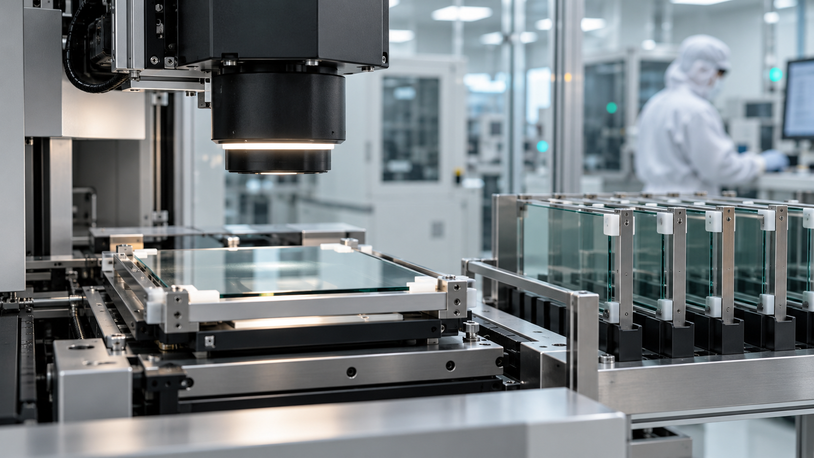
These are proposed engineering criteria for interpreting industrialization. They are not measured shortcomings of the disclosed routes. Evidence becomes stronger when it connects substrate-scale processing with defined device acceptance results and repeated operation.
Throughput belongs in that assessment too. A process may add, combine, or remove operations. The number of steps alone does not establish the cost per acceptable panel. Time, materials, equipment use, maintenance, and rejected output affect the result. Public descriptions without those data cannot support an invented cost or yield figure.
Inspection must follow the new process risks. If patterning relies on selective removal, the evaluation should address the resulting boundaries and any effect on the remaining material. If protection is central, the evidence should establish its performance through subsequent operations. The exact test method depends on the disclosed product and available technical documentation.
Distinguish disclosure, demonstration, and product qualification
The published evidence supports interest in several manufacturing routes. It also requires precise descriptions of what each source establishes. A technical disclosure explains an approach. A demonstration shows a result under stated conditions. Qualification connects an actual product to defined requirements.
The LG announcements provide a dated account of FLiPP and its reported processing. The Applied Materials release provides a dated equipment-platform announcement and evaluation milestone. The research paper provides experimental device evidence. These sources answer different questions; they cannot be added together as proof of completed mass production for an unspecified panel.
For an OEM technology roadmap, the next useful milestone is evidence tied to a particular product category and complete display. That allows the team to connect manufacturing progress with relevant electrical, optical, environmental, and integration requirements.
Patterning is also a separate axis from vertical emissive-stack architecture. A tandem description concerns how emissive units are stacked through the device. FMM-less pixel patterning concerns lateral placement across the display. One label does not establish the other.
Bring the process claim back to the complete assembly
OEM teams can use FMM-less disclosures to understand which manufacturing constraints developers are addressing. The commercial assembly still determines what the equipment can use. A process innovation does not by itself establish mounting, host compatibility, power requirements, or support arrangements.
For broader terminology, RJY’s TFT, OLED, and LCD overview provides a separate starting point. The process analysis here concerns how emissive regions are formed, rather than a universal verdict on display technologies.
For existing LCD products, RJYディスプレイ can discuss selected TFT LCD and controller integration. Any alternative platform needs verified assembly documentation. FMM-less OLED patterning deserves attention because it changes manufacturing choices; its product value emerges when those choices produce a repeatable, qualified display.
よくある質問
Does FMM-less mean that the factory uses no masks?
No. It refers to reduced dependence on a fine metal mask at the relevant patterning step. Other deposition masks, fixtures, or lithographic operations can remain in the process.
Is FMM-less OLED the same as inkjet printing?
No. The label does not specify the replacement method. Identify how the disclosed route forms the emissive regions and protects the material through later operations.
Does better glass utilization establish a higher factory yield?
No. Glass layout utilization describes the use of substrate area. Device yield concerns the proportion that meets defined acceptance criteria. Compare each metric using its own stated denominator and conditions.
参考文献
- Display terminology: FMM (Fine Metal Mask). Samsung Display, December 8, 2020.
- Display terminology: Open Mask. Samsung Display, December 23, 2020.
- FLiPP introduction at IMID 2026. LG Display, August 19, 2026.
- FLiPP technology seminar report. LG Display, October 11, 2026.
- Applied Materials Breakthrough To Bring OLED Displays to Tablets, PCs and TVs. Applied Materials, November 21, 2024.
- Micrometer-scale indirect photopatterning of RGB OLED emissive layers in single phase network structure. Light: Science & Applications, July 22, 2025.