FMM-less OLED patterning changes how manufacturers place the red, green, and blue emissive regions across a display. Its purpose is to form useful pixel structures while reducing dependence on a fine metal mask at the relevant patterning step. The engineering challenge is to preserve the OLED materials as well as the intended geometry.
Public disclosures describe several routes toward that goal. They differ in deposition, protection, selective pattern formation, and encapsulation. Understanding those differences matters more than treating “maskless” as one manufacturing recipe. This analysis examines the public evidence available as of October 20, 2026, then explains the process questions that determine scale-up.
Fine metal masks place deposited material at subpixel locations
A fine metal mask, or FMM, is a thin metal plate with small openings. In the deposition approach described by Samsung Display, those openings guide evaporated organic material to the intended subpixel positions. Different color-specific masks support sequential red, green, and blue deposition.[1]
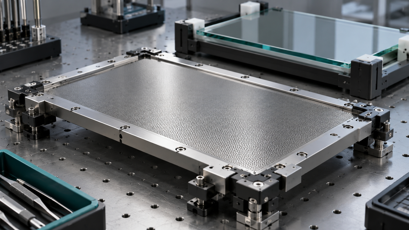
The mask therefore performs a geometric task inside a material-deposition process. Its openings, position, and relationship to the substrate influence where material arrives. The process must preserve that relationship over the area being patterned.
Larger masks can sag or warp, changing alignment with the substrate.[3] A gap between the mask and substrate can also create a shadow region at an opening, affecting fine-feature fidelity.[6] The resulting limits depend on the process and equipment.
It also helps to distinguish fine patterning from broad-area coating. Samsung Display separately describes open masks for deposition over larger display areas or common layers.[2] The direct-RGB approach is one color-formation route, rather than a description of every OLED process. Removing an FMM from a particular step does not remove every mask, fixture, or lithographic operation from the factory.
FMM-less routes transfer the patterning task to other process steps
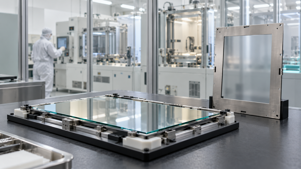
The useful question is what replaces the FMM’s geometric function. A process still needs to select where emissive material remains, where another color can form, and how neighboring regions stay distinct. It must also protect the material already in place.
LG Display introduced FLiPP, its FMM-Less innovative Pixel Patterning technology, at IMID in August 2026. Its public description combines deposition or coating with protection, pattern removal, and photolithography. The company also reported processing full generation-8.5 mother glass in its implementation.[3]
An October 11, 2026 Korean-language LG Display report described an October 8 seminar. It outlined successive RGB processing involving deposition, encapsulation or a protective film, and photo-patterning with a UV-related removal step.[4] This is a public process outline, rather than the complete conditions needed to reproduce it.
The central trade-off changes location. The process can reduce reliance on a fine metal mask while increasing the importance of selective pattern formation, protection, and removal. The overall result depends on how those operations work together, not simply on the absence of one tool.
Compare public routes by their stated process function
Applied Materials announced MAX OLED in November 2024. Its description combines a patented pixel architecture with maskless selective deposition and individual pixel encapsulation. It presents deposition, encapsulation, and materials handling as an integrated equipment approach. The release said Applied would supply an alpha system to Samsung Display to assess the technology.[5]
That date establishes an announced evaluation plan. It does not establish the system’s present deployment stage. Equally, an equipment platform and a qualified finished panel represent different products and different evidence.
| Public route | Emphasis in the disclosure | Useful interpretation |
|---|---|---|
| LG Display FLiPP | Protected organic-layer processing and photo-patterning | Examine how selective formation and material protection work across successive colors. |
| Applied Materials MAX OLED | Selective deposition, pixel architecture, and individual pixel encapsulation | Examine the integrated process and the evidence for the intended panel application. |
| Academic indirect photopatterning | A laboratory method to form emissive patterns while limiting direct processing damage | Use it to understand material constraints and device validation. |
The comparison describes the public approaches; it does not rank them or establish common intellectual property. Nor does FMM-less identify inkjet printing by definition. The term identifies a process dependency that has changed, while the replacement method needs its own description.
Pattern fidelity matters only if the organic device still works
A clean-looking pattern is an intermediate result. The patterned organic material must retain the electrical and optical behavior needed in the finished device. Processes that expose materials to light, chemicals, or removal steps therefore require more than geometric inspection.
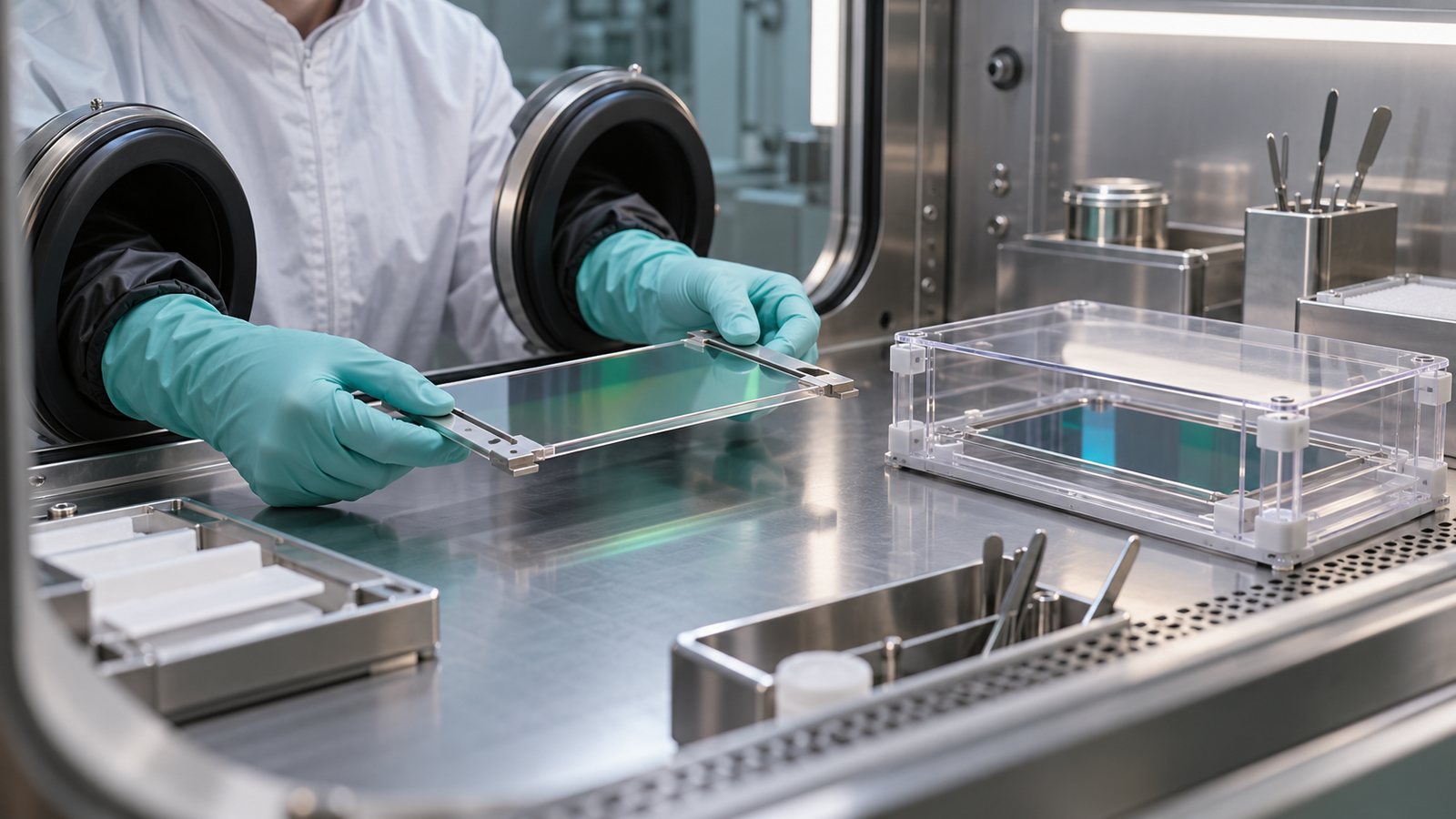
A July 2025 paper in Light: Science & Applications demonstrated indirect photopatterning of solution-processed RGB emissive layers. The research used a sacrificial photoresist and network formation to reduce direct exposure to damaging processing conditions. It addresses the sensitivity of organic emissive materials to UV, solvents, and etching.[6]
The study is a laboratory demonstration. It helps explain why material protection is a core engineering problem, but it does not identify the proprietary process used by LG Display or Applied Materials.
Our proposed evaluation begins with the device after patterning. Compare its electrical behavior, light output, color, and aging with a suitable reference. Then assess pattern boundaries, uniformity, and the effect of processing adjacent colors. A successful shape and a successful OLED device are related results that require separate evidence.
Residual material and contamination also deserve attention in process development. These are areas to inspect, rather than allegations about a named commercial technology. The aim is to establish that the complete sequence preserves function repeatedly.
Separate aperture, material use, glass layout, and device yield
Manufacturing announcements can report several improvements together. The metrics may all be useful, but they measure different things. Combining them into a single “efficiency” claim loses the denominator that gives each result meaning.
| Metric | What it relates | What it cannot establish alone |
|---|---|---|
| Emitting aperture fraction | The emitting area relative to the reference area defined in the report | The complete display’s power or lifetime at an unspecified operating point |
| Deposition material utilization | Useful material deposition relative to material input, under the stated definition | The fraction of completed panels that meet acceptance requirements |
| Glass cutting or layout utilization | The use of mother-glass area for a stated panel layout | The rate of electrically and optically acceptable devices |
| Acceptable-device yield | Devices meeting defined acceptance criteria relative to the relevant production population | A result transferable to every size, design, or production stage |
LG’s October report discusses aperture, cutting utilization, and deposition material utilization as separate measures.[4] Keeping them separate is essential when interpreting the manufacturing argument.
Each metric can support a different design or business decision. A larger emitting fraction can create room for optical or electrical trade-offs. Better material use can affect a process input. A more effective cutting layout concerns the arrangement of panels on glass. None supplies a factory good-panel rate by itself.
For the same reason, a larger aperture does not automatically produce a universal power saving. The final result depends on the selected brightness, driving conditions, optical structure, and other parts of the design.
Scale-up needs repeatability across area and over time
A small patterned region can demonstrate a mechanism. A larger substrate tests additional demands: alignment over distance, uniform processing, handling, inspection coverage, and consistency among regions. A production process must also repeat those results over time.
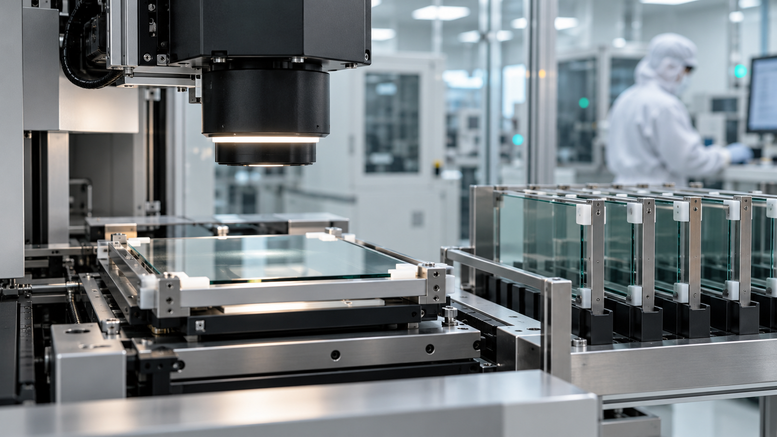
These are proposed engineering criteria for interpreting industrialization. They are not measured shortcomings of the disclosed routes. Evidence becomes stronger when it connects substrate-scale processing with defined device acceptance results and repeated operation.
Throughput belongs in that assessment too. A process may add, combine, or remove operations. The number of steps alone does not establish the cost per acceptable panel. Time, materials, equipment use, maintenance, and rejected output affect the result. Public descriptions without those data cannot support an invented cost or yield figure.
Inspection must follow the new process risks. If patterning relies on selective removal, the evaluation should address the resulting boundaries and any effect on the remaining material. If protection is central, the evidence should establish its performance through subsequent operations. The exact test method depends on the disclosed product and available technical documentation.
Distinguish disclosure, demonstration, and product qualification
The published evidence supports interest in several manufacturing routes. It also requires precise descriptions of what each source establishes. A technical disclosure explains an approach. A demonstration shows a result under stated conditions. Qualification connects an actual product to defined requirements.
The LG announcements provide a dated account of FLiPP and its reported processing. The Applied Materials release provides a dated equipment-platform announcement and evaluation milestone. The research paper provides experimental device evidence. These sources answer different questions; they cannot be added together as proof of completed mass production for an unspecified panel.
For an OEM technology roadmap, the next useful milestone is evidence tied to a particular product category and complete display. That allows the team to connect manufacturing progress with relevant electrical, optical, environmental, and integration requirements.
Patterning is also a separate axis from vertical emissive-stack architecture. A tandem description concerns how emissive units are stacked through the device. FMM-less pixel patterning concerns lateral placement across the display. One label does not establish the other.
Bring the process claim back to the complete assembly
OEM teams can use FMM-less disclosures to understand which manufacturing constraints developers are addressing. The commercial assembly still determines what the equipment can use. A process innovation does not by itself establish mounting, host compatibility, power requirements, or support arrangements.
For broader terminology, RJY’s TFT, OLED, and LCD overview provides a separate starting point. The process analysis here concerns how emissive regions are formed, rather than a universal verdict on display technologies.
For existing LCD products, RJY Display can discuss selected TFT LCD and controller integration. Any alternative platform needs verified assembly documentation. FMM-less OLED patterning deserves attention because it changes manufacturing choices; its product value emerges when those choices produce a repeatable, qualified display.
Frequently asked questions
Does FMM-less mean that the factory uses no masks?
No. It refers to reduced dependence on a fine metal mask at the relevant patterning step. Other deposition masks, fixtures, or lithographic operations can remain in the process.
Is FMM-less OLED the same as inkjet printing?
No. The label does not specify the replacement method. Identify how the disclosed route forms the emissive regions and protects the material through later operations.
Does better glass utilization establish a higher factory yield?
No. Glass layout utilization describes the use of substrate area. Device yield concerns the proportion that meets defined acceptance criteria. Compare each metric using its own stated denominator and conditions.
References
- Display terminology: FMM (Fine Metal Mask). Samsung Display, December 8, 2020.
- Display terminology: Open Mask. Samsung Display, December 23, 2020.
- FLiPP introduction at IMID 2026. LG Display, August 19, 2026.
- FLiPP technology seminar report. LG Display, October 11, 2026.
- Applied Materials Breakthrough To Bring OLED Displays to Tablets, PCs and TVs. Applied Materials, November 21, 2024.
- Micrometer-scale indirect photopatterning of RGB OLED emissive layers in single phase network structure. Light: Science & Applications, July 22, 2025.