Facing a bottleneck in your Embedded Display Project?
Don’t let complex integration or supply chain issues slow your time-to-market. Book a free consultation with the RJY expert team for tailored design and manufacturing support.

A MIPI display interface can connect a compact embedded processor to a high-resolution LCD with only a small number of high-speed signal lanes. An LVDS interface display module can fit an industrial mainboard that already produces continuous LVDS pixel data. Neither interface is automatically better, and neither interface name proves that a panel will work with a particular host.
The correct choice depends on the complete display path: processor output, panel input, resolution, timing, color format, lane or channel configuration, initialization, power sequence, backlight, touch connection, PCB layout, cable, firmware, and operating environment. A 1920×720 display, for example, cannot be classified as single-channel LVDS, dual-channel LVDS, or a fixed MIPI lane count from resolution alone.
This guide compares MIPI DSI and LVDS from an industrial product-development perspective. It explains what engineers need to verify before choosing a panel, designing a controller board, or ordering samples.
In a display project, “MIPI interface” usually refers to the MIPI Display Serial Interface, or MIPI DSI. The MIPI Alliance developed DSI to carry image data and display-control traffic between a host processor and a display peripheral. Current DSI-2 specifications can use MIPI D-PHY or C-PHY physical layers and support several operating modes.1
A typical embedded path includes:
MIPI DSI commonly uses one clock lane and one or more data lanes with D-PHY, although the exact architecture depends on the specification version and hardware. The host and display must support the same physical configuration, operating mode, data format, rate, and command set.
In Video Mode, the host sends a continuous stream that follows the required display timing. This behavior resembles a conventional raster video path. In Command Mode, the host sends commands and image updates to a display that can manage image memory or update behavior internally. Support depends on both the host and the panel driver IC.
The labels are not interchangeable configuration options. A panel designed for one mode may need a specific sequence of registers, packet types, lane states, and timing values. The MIPI Alliance describes DSI-2 as supporting video, graphical-user-interface command, and static operating modes, but an individual product implements only the features stated in its documentation.1
DSI and CSI-2 use related MIPI physical-layer technology, but they serve different data paths. DSI sends information toward a display. CSI-2 commonly transports image data from a camera or image sensor toward a processor. A board with a camera connector does not therefore have a usable display output merely because both connectors are called MIPI.
LVDS means low-voltage differential signaling. In many LCD systems, an LVDS transmitter serializes parallel pixel information and sends it over several differential pairs. A receiver in the display timing controller reconstructs the pixel data and clock.
An LVDS display module may use a single-channel or dual-channel architecture. The terms describe how pixel information is divided across the link, but they do not define every electrical or logical detail. Designers must also confirm:
Descriptions such as “40-pin LVDS” or “dual-channel LVDS” are incomplete. Two panels can use the same connector family and still assign power, ground, signals, or control pins differently. Connecting them without checking both datasheets can prevent operation or damage hardware.
| Design factor | MIPI DSI | LVDS panel interface |
|---|---|---|
| Common host context | Embedded SoC with native DSI output | Industrial mainboard, display controller, or bridge with LVDS output |
| Link structure | Packet-based display protocol over a MIPI physical layer | Serialized pixel and timing data over differential pairs |
| Configuration terms | Lane count, data rate, mode, packet format, commands | Channel count, mapping, clock, color depth, timing |
| Initialization | Often needs panel-specific commands and register settings | May rely more on continuous timing but still needs correct power and control behavior |
| Physical integration | Often used for compact PCB-to-FPC paths | Often used through a defined cable or board-to-panel harness |
| Conversion | Requires an active bridge if the source is not native DSI | Requires an active transmitter or bridge if the source is not native LVDS |
The comparison does not mean that every DSI design is short, every LVDS design is long, or one technology is always more reliable. Data rate, PCB stack-up, cable construction, connector, electromagnetic environment, source capability, and receiver tolerance determine the practical implementation.
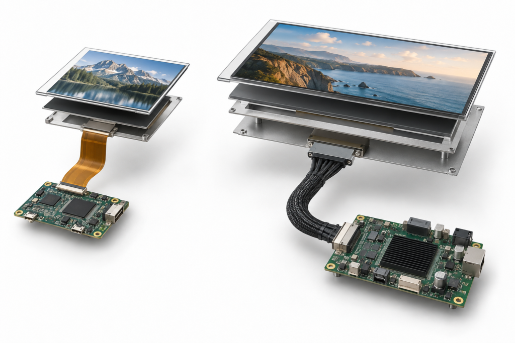
A connector is only a mechanical component. It does not define the display protocol or pin assignment. Product teams often find a panel with the same pin count and assume it can replace the original. This assumption can fail for several reasons:
Even a verified electrical pinout is not enough. The host must produce the panel’s resolution, timing, data format, and initialization. A panel can remain black while its backlight is operating because the image interface has not started correctly.
Resolution affects the required data rate, but it is only one input. A first estimate of active image data is:
horizontal pixels × vertical pixels × refresh rate × bits per pixel
This estimate excludes horizontal and vertical blanking, packet overhead, encoding, control traffic, and link margin. It also assumes uncompressed image data. The actual design must use the complete timing table and the rules of the selected interface.
For example, two panels with the same 1920×720 active resolution may specify different total horizontal periods, total vertical periods, refresh rates, color depths, and pixel clocks. One may use a particular dual-channel LVDS mapping, while another uses a different interface or channel arrangement. The visible pixel count does not settle the link design.
The pixel clock relates to the total number of transmitted pixel periods, not only the visible pixels. Each line can contain front porch, synchronization, and back porch intervals. Each frame can include similar vertical intervals. A controller that produces the correct active resolution but the wrong total timing may cause a shifted, unstable, partial, or blank image.
A 24-bit RGB path carries more active color information than an 18-bit path. Host and panel must agree on the format. An incorrect format or mapping can produce wrong colors even when the image geometry looks correct.
A 1920×720 LVDS display has a wide aspect ratio that can suit instrument panels, control consoles, vehicle interfaces, bar-type HMIs, and information systems. That application fit does not define the exact electrical configuration. Engineers must review the panel datasheet before choosing a mainboard or controller.
Record the active area, total horizontal and vertical periods, synchronization widths, porches, refresh range, pixel clock, and any required polarity. Use the typical values for initial setup and verify the allowed minimum and maximum ranges. Do not configure a controller from the visible resolution alone.

Do not assume that every 1920×720 module needs dual-channel LVDS. The panel datasheet defines the channel structure. If dual-channel operation is specified, the host must distribute the pixels in the required order. A mismatch can create split, repeated, interleaved, or color-corrupted images.
Bit mapping also matters. Terms such as JEIDA and VESA appear in LCD integration work, but the correct mapping must come from the specific transmitter and panel documentation. A mapping mismatch commonly changes colors or bit significance.
A 1920×720 canvas is not a normal 16:9 desktop layout. The interface should place critical information where users can read it at the intended distance and angle. A stretched conventional UI may waste the width, make controls too small, or force important content toward an inaccessible edge.
The wide module may require a backlight driver, connector, cable route, mounting frame, and thermal path that differ from those of a smaller screen. Confirm LED voltage and current requirements, dimming method, startup behavior, and mechanical support from the panel documentation. Do not power the backlight directly from a signal interface.
MIPI DSI is a strong candidate when the host processor provides a native DSI output and the display sits close to the processor in a compact product. It is common in handheld, smart-home, robotic, appliance, and other embedded devices built around integrated application processors.
A practical MIPI project usually has these conditions:
A native DSI output can reduce the need for a separate video bridge. However, the implementation may require more firmware and panel-specific initialization work than a buyer expects from the connector count alone.
LVDS remains useful when an industrial mainboard, single-board computer, or display controller already provides a compatible LVDS output. Many established industrial systems use LVDS because the processor, BIOS, cable, and panel ecosystem were designed around it.
An LVDS panel is a practical candidate when:
LVDS is not automatically plug-and-play. Industrial mainboards often offer several LVDS settings, and an incorrect BIOS profile can produce no image or an unstable image. The board specification must also distinguish its internal LVDS output from external interfaces such as HDMI or DisplayPort.
MIPI DSI and LVDS use high-speed differential signaling. A schematic connection that is logically correct can still fail when the physical design degrades the signal.
Use the impedance target, geometry, spacing, and material data required by the relevant component and PCB design. Keep each positive and negative trace within a pair closely matched. Control discontinuities at vias, connectors, test points, and layer changes.
Excess difference in propagation delay can reduce timing margin. The permitted mismatch depends on the data rate and interface implementation. Follow the host, bridge, connector, and panel design guides rather than applying one universal length rule.
High-speed current needs a continuous reference path. Plane gaps, poor connector grounding, long stubs, and noisy power regions can increase emissions or reduce signal quality. Keep switching regulators, backlight nodes, radios, motors, and other noise sources in mind when placing the display path.
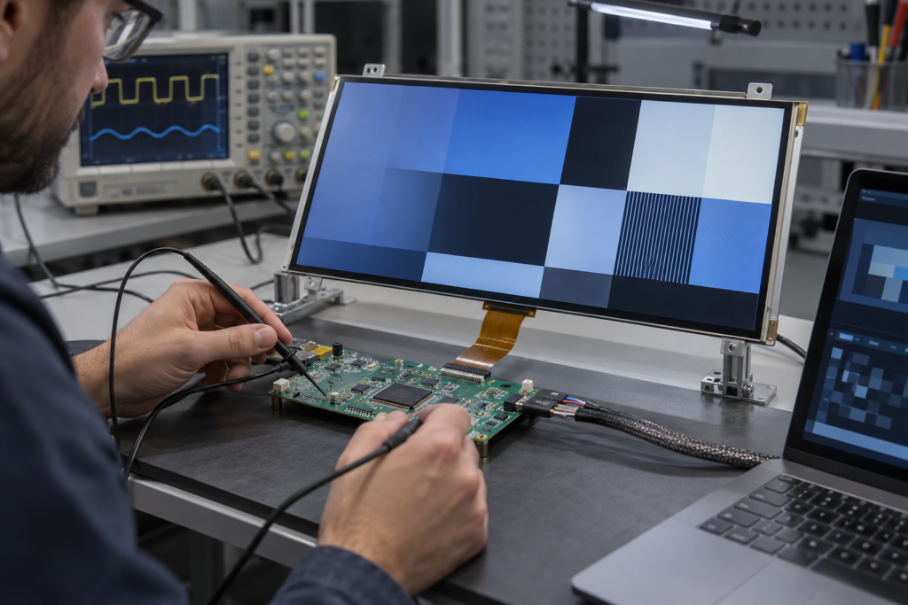
A bench prototype with a short FPC does not prove that a longer production harness will work. Test the chosen cable, bend radius, connector, enclosure, temperature, and nearby noise sources. If the project needs a long in-vehicle or factory link, a local panel interface may not be the only transport technology required.
A display can fail even when its data lanes are routed correctly. Many panels require a defined order for logic power, analog rails, reset, interface activity, display enable, and backlight. Sleep and wake can use a different sequence.
MIPI DSI panels often need a list of vendor-specific commands. These commands can configure orientation, pixel format, porch values, internal power circuits, gamma behavior, sleep exit, and display enable. A driver IC name alone may not provide the correct sequence because the panel manufacturer can configure the IC for a particular glass and module.
An LVDS panel may not need the same command path, but the source still needs the correct pixel timing and control state. Backlight operation should begin only after the image path is ready when the panel documentation requires that order. Otherwise, the user may see a bright blank screen, flash, or unstable startup.
MIPI DSI or LVDS carries display information. It does not automatically provide touch data or backlight power.
| Function | Common path | What must be checked |
|---|---|---|
| Image | MIPI DSI or LVDS | Timing, format, lanes or channels, initialization |
| Capacitive touch | I²C or USB | Touch IC, voltage, interrupt, reset, driver, coordinate mapping |
| Backlight | LED driver and power path | Voltage, current, dimming, enable, thermal design |
| Panel control | GPIO, I²C, SPI, or DSI commands | Reset, enable, initialization, sleep and wake |
This separation matters during controller-board selection. An HDMI input board may produce the panel image while a USB connection returns touch data to the host. The board may also need a separate LED driver. “HDMI touchscreen” is therefore a system description, not evidence that HDMI carries every signal.
A host with native DSI can connect to a compatible panel without converting from another video standard. The team still needs to implement the correct lane arrangement, electrical design, timing, commands, power sequence, and software driver.
A mainboard with a compatible LVDS transmitter can connect to an LVDS panel through a verified cable. The team must configure channel count, mapping, timing, voltage, and backlight. Board menu options or connector shape do not replace the panel review.
If the host provides HDMI, eDP, RGB, or another source, a bridge or controller board must receive that source and generate the exact panel output. HDMI-to-MIPI is an active conversion. The bridge firmware must contain the panel timing and initialization. A board made for one MIPI panel should not be assumed to support another panel.
The same principle applies to other conversions. A bridge chip’s data sheet may show that a signal path is technically possible, but a production board still needs power, clocks, memory if required, connectors, firmware, layout, thermal design, and validation. See the RJY HDMI-to-MIPI compatibility guide for the information needed before board selection.
| Symptom | Areas to check |
|---|---|
| Completely black screen | Power rails, reset, initialization, lane assignment, host mode, FPC orientation |
| Backlight on but no image | DSI traffic, panel commands, video timing, sleep exit, display enable |
| Wrong colors | Pixel format, RGB order, color depth, lane configuration, driver settings |
| Shifted or cropped image | Active area, porch values, sync timing, orientation, scaling |
| Intermittent lines or flicker | Signal integrity, power noise, data rate, connector contact, clock stability |
| Works at boot but not after sleep | Wake commands, reset state, power sequence, host driver recovery |
These are investigation paths, not remote diagnoses. Capture the hardware revision, firmware version, oscilloscope or protocol evidence where available, and the exact conditions that reproduce the fault.
LVDS failures often come from configuration mismatches:
Test patterns can help separate geometry, mapping, and color problems. Backlighting the panel and inspecting it at an angle can help determine whether image data exists when the backlight is not operating. Follow safe electrical procedures and the module documentation.
This process may show that the easiest path is to select a panel with the host’s native interface. In other projects, a bridge board is justified because mechanical, optical, or supply requirements make a particular panel valuable.
Provide the following information before requesting a panel or controller-board recommendation:
If the current panel is unavailable, include its mechanical drawing and optical requirements as well as the electrical data. A replacement must fit the enclosure and viewing area, not only the host interface.
RJY Display can review project-specific customization based mainly on existing display modules. Depending on the selected module and project scope, the work may include:
Customization does not mean that any panel can be converted to any interface or that a completely new LCD size can be developed for every project. Feasibility depends on the existing display platform, host architecture, project volume, schedule, and engineering requirements.
MIPI DSI and LVDS are not isolated labels on an LCD catalog. They connect a host, physical link, display electronics, power system, firmware, and mechanical assembly. A successful project matches every part of that path.
Start with the host output and panel datasheet. Calculate the data requirement from complete timing, not active resolution alone. Verify the MIPI lanes and commands or the LVDS channels and mapping. Then validate power, backlight, touch, cable, PCB layout, firmware, and enclosure under real operating conditions.
For more background, see the RJY LCD display interface guide. If you are selecting an industrial LCD panel or matching a controller board, contact RJY Display with the panel and host documentation for an engineering review.
In an LCD project, the term usually means MIPI DSI, a serial display interface between a host processor and a display peripheral. Compatibility depends on the physical layer, lane count, operating mode, data rate, timing, panel commands, and electrical design.
No. DSI is designed for display communication, while CSI-2 is commonly used for camera and image-sensor data. They may use related physical-layer technology, but their protocols and system roles differ.
Not in every project. MIPI DSI may fit a compact SoC-based design with native DSI output. LVDS may fit an industrial mainboard that already supports the required LVDS timing and mapping. The host, panel, firmware, cable, and environment determine the better choice.
Not directly. An active bridge or controller must convert the source into the exact MIPI DSI lane configuration, timing, data format, and initialization required by the panel. Compatibility must be confirmed for the specific devices.
No. Panels with the same pin count can use different voltages, signal assignments, lane or channel configurations, backlight connections, and initialization. Compare the complete pin definitions and datasheets.
Resolution alone cannot answer this. The required channel count depends on the panel design, pixel clock, refresh rate, color depth, timing, and receiver architecture. Use the exact panel datasheet.
The display interface normally carries image data. A capacitive touch controller commonly uses a separate I²C or USB connection, with additional interrupt, reset, power, and driver requirements.
Provide the panel model, datasheet, resolution, complete timing, interface, pin definition, driver IC, backlight information, touch requirements, host source, operating system, firmware needs, mechanical constraints, and operating environment.
MIPI is a registered trademark of MIPI Alliance, Inc. Interface names and third-party trademarks are used for technical identification only.
Share your display size, resolution, interface, brightness, touch requirement, controller board requirement, and application environment.
Continue reading related display technology guides and application references.
Talk to RJY’s engineering team for display matching, controller board review, and customization discussion.