A CPU can finish drawing a TFT image while DMA or LTDC still reads old pixels. On a Cortex-M7 STM32 design using cacheable write-back memory, the latest CPU writes may remain in dirty cache lines rather than in the memory visible to the display-side reader. Finishing the draw operation and publishing its results are separate events.
The driver must also protect the buffer after publication. Cleaning a cache range does not authorize the CPU to overwrite pixels that a transfer or scanout engine still uses. This article examines that handoff for CPU-produced buffers on relevant STM32F7/H7 designs. It does not provide a receive-DMA recipe, a universal STM32 memory map, or hardware test results.
Separate rendering, visibility, and release
Three questions identify the handoff. Has the CPU finished writing the intended pixels? Can the selected hardware reader observe those writes? Has that reader stopped using the buffer? A correct answer to one question does not answer the others.
For CPU-written source data in write-back memory, ST AN4839 describes cache maintenance needed for DMA visibility and distinguishes cleaning from invalidation. Cleaning writes dirty data back toward memory; the target sequence must make it visible to the selected reader. Invalidating alone can discard dirty CPU updates instead of publishing them.[1]
Consider an illustrative buffer containing an old image. The CPU draws a marker into its cached copy. A memory-reading device can still obtain the old image if the new data has not reached the memory it observes. The CPU reading back its own marker does not prove that the device sees it; both CPU operations may use the same cache.
This explanation assumes that the reader does not automatically obtain the CPU’s dirty cache contents through a coherent path. Verify the actual target architecture rather than applying the assumption to every processor or interconnect.
Check the memory path before choosing maintenance
Start with the exact MCU, buffer allocation, and reader. Determine whether that DMA engine or LTDC can access the allocated memory through the target’s bus structure. Then establish the effective memory attributes, including MPU configuration and cache policy. A buffer address by itself does not answer either question.
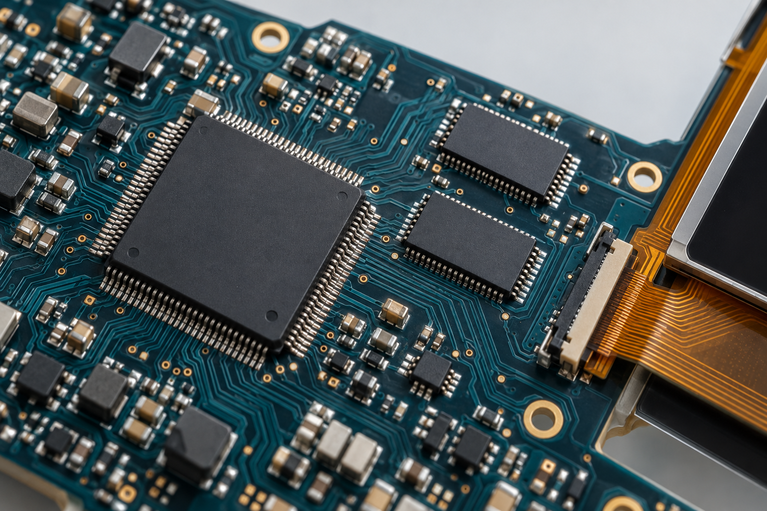
Do not generalize that a named RAM region is accessible to every STM32 DMA engine. Likewise, a linker section called framebuffer does not establish a cache policy. Compare the linker placement with the runtime configuration and the reference manual for the selected part.
A deliberately non-cacheable region can change the visibility problem, but it is a design choice with performance and configuration consequences. It does not remove ownership rules. Disabling the whole cache may change a symptom during diagnosis; that observation does not establish the cause or a suitable production fix.
ST’s Cortex-M7 recommendations for LTDC address coordination between cache behavior and display memory access. Their scope is target-specific; cache maintenance can itself affect access to shared memory.[2] Avoid turning that guidance into a universal framebuffer location or timing prescription.
Publish the final CPU writes before the reader starts
The following sequence is an integration model, not portable driver code. Complete the CPU’s writes to the source buffer. Prevent all producers, including interrupt callbacks, from modifying it during the handoff. Perform the cache maintenance required by its policy and the target software. Complete the target’s required ordering and maintenance sequence. Then submit or expose the buffer to the reader.
A late CPU write breaks that sequence. If the application cleans a buffer and then modifies a status icon before starting DMA, the icon can remain unpublished. The cache operation must cover the final data for that handoff, not merely an earlier version of the frame.
Marking the buffer volatile does not clean dirty cache lines. A barrier also does not substitute for a clean operation. The correct ordering and completion instructions belong to the target API and driver contract; they must accompany the required data publication rather than replace it.
For a controlled investigation, record the last rendering event, maintenance range, submission event, and completion event. This provides more useful evidence than scattering maintenance calls through drawing functions and observing whether the screen looks better.
Account for cache lines beyond the requested pixels
The Arm CMSIS-Core 5.6.0 M7 documentation specifies a 32-byte aligned start address and a byte count for its by-address maintenance functions. Check the project’s CMSIS implementation and preconditions before using an example from another version.[3]

As an arithmetic teaching case, assume a 50-byte dirty region starts at the fictional address 0x20000013. With 32-byte maintenance granularity, rounding the start down and the exclusive end up produces:
| Menge | Veranschaulichender Wert |
|---|---|
| Requested start | 0x20000013 |
| Requested length | 50 bytes |
| Requested exclusive end | 0x20000045 |
| Aligned start | 0x20000000 |
| Aligned exclusive end | 0x20000060 |
| Covered maintenance span | 96 bytes |
The expanded span includes neighboring bytes. Allocation and ownership must account for that fact, especially if unrelated objects share a cache line. This example assumes that all 96 bytes lie within one valid allocation under the same exclusive ownership until handoff. A clean can write back neighboring dirty bytes, so sharing a cache line with an unrelated writer requires a separate ownership design. Aligning a range for an API call is not proof that every affected byte belongs to the caller. Moving the start down while still passing the original 50-byte count would not cover the full intended range; the calculated span here is 96 bytes.
The arithmetic assumes a nonempty region and valid address calculations. Production range handling must check overflow, length limits, accessible allocation boundaries, and API-specific requirements. The example address does not identify a memory region accessible to any particular STM32 device.
Partial image updates need the same discipline. Identify every CPU-written memory range that the reader will consume. A dirty rectangle can span several separated row ranges; its visible dimensions alone do not define one contiguous byte interval. Use the established allocation layout without repeating a pixel-format conversion as a cache fix.
Keep a published buffer unchanged until valid release
Publication establishes visibility of a particular set of writes. Ownership establishes who may change the buffer next. The CPU should not resume writing merely because a clean call returned or a transfer was queued.
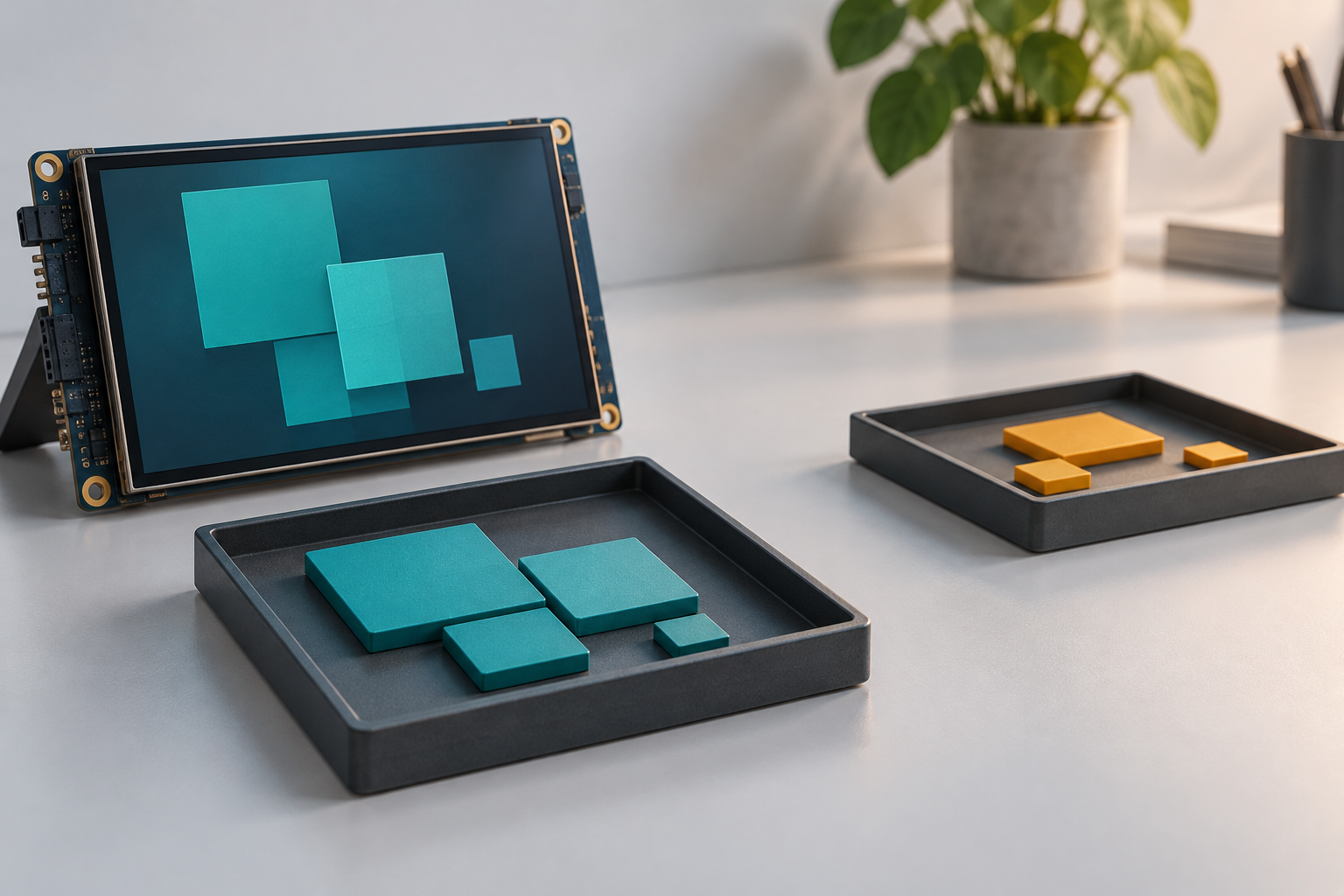
| Illustrative state | Permitted action | Required transition evidence |
|---|---|---|
| CPU owns writable buffer | Render the next content | Rendering completes |
| Ready for publication | Publish final writes using target requirements | Required maintenance and ordering complete |
| Reader owns source | Transfer or scan out unchanged content | Reader-specific release event |
| Released | Return buffer to the writable pool | Driver records ownership change |
A one-shot transfer and continuous LTDC scanout need different release definitions. For a transfer source, the relevant completion must mean that the hardware no longer reads it. For scanout, a submitted address change does not alone prove that the previous framebuffer is free. The driver must establish when the display engine has switched away under the target’s documented lifecycle.
Double buffering helps only when this lifecycle is correct. Two allocations do not prevent the renderer from selecting a buffer still in use. Record which buffer is writable, queued, active, and released, and make those states agree with the actual driver events.
Connect the GUI completion signal to actual reuse
In LVGL 9.5, lv_display_flush_ready() reports flush completion so LVGL can reuse the draw buffer. For an asynchronous transfer from that buffer, report completion only after the driver knows the reader has finished. A custom flush-wait callback offers another documented mechanism.[4]
The integration must define what the flush operation does with its input. If it copies into another owned buffer, the original and destination can have different release events. If the display engine reads the original directly, its lifetime must cover that read. Neither case should be inferred from the callback name alone.
Reporting completion immediately after starting DMA can allow the renderer to overwrite the source mid-transfer. Waiting for a CPU copy to finish can release its source while the destination remains active. Map the GUI’s completion contract onto these actual relationships and the installed library version.
Use observations to choose the next investigation
| Beobachtung | Nächste zu sammelnde Nachweise |
|---|---|
| CPU sees new pixels while display shows old regions | Effective cache policy, final write timing, and published range |
| Changes after publication disappear or arrive late | Writes made after clean and ownership transitions |
| Image mixes content from different updates | Reuse events and active-reader lifetime |
| Behavior changes when cache is disabled | Memory-path and publication evidence; do not declare a final fix |
| Corruption remains with stable, published, owned buffers | Other layers, including bandwidth, layout, and interface timing |
These observations are clues, not unique diagnoses. A stale-looking region can have more than one cause. A synthetic RAM/cache model can demonstrate why publication matters, but it cannot establish memory accessibility, bus timing, or interrupt behavior on a board.
You can reproduce the range calculation without a board: add 50 to 0x20000013, round the start down and the exclusive end up to 32-byte boundaries, then subtract. The result is 96 bytes. This arithmetic does not execute CMSIS or validate hardware cache maintenance.
Once visibility and ownership are documented, investigate other layers on their own evidence. RJY’s LCD pixel clock and display timing guide covers link timing. Its LCD display module interfaces guide provides interface context. Changing those layers does not publish a dirty CPU cache line.
Provide the handoff evidence for integration review
For a scoped discussion, kontaktieren Sie RJY Display with the MCU part, memory placement and MPU policy, display interface, resolution and pixel format, driver handoff sequence, and observed failure. Include exact panel and controller data and the software versions. Project-specific module or board review can then address the documented integration boundary without assuming universal compatibility.