Facing a bottleneck in your Embedded Display Project?
Don’t let complex integration or supply chain issues slow your time-to-market. Book a free consultation with the RJY expert team for tailored design and manufacturing support.

An LVDS TFT LCD can power up, lock to the incoming signal, and show a stable image while still rendering colors incorrectly. When resolution and synchronization look correct but gradients are posterized, dark tones are crushed, or colors appear unnaturally shifted, the problem may be the data mapping rather than the panel glass, cable quality, or application software.
VESA and JEIDA are commonly referenced mapping conventions for arranging RGB pixel bits across an LVDS display link. They do not change the physical connector by themselves, and they should not be confused with pixel timing, lane polarity, single- versus dual-channel LVDS, or the electrical characteristics of the interface. They define how the transmitter and receiver interpret the serialized pixel data. Both ends must agree.
This guide explains how mapping affects an embedded TFT LCD system, how to distinguish a mapping problem from other compatibility failures, and what engineers should verify before approving a replacement panel or controller-board configuration.
LVDS describes a low-voltage differential signaling method, but an LCD connection also needs an agreed method for transporting pixel and control information. In many flat-panel systems, a serializer converts parallel RGB data into a stream carried over differential pairs, and the panel-side receiver reconstructs the pixel data.
Texas Instruments documents multiple RGB-to-LVDS/OpenLDI mappings for 18-bit and 24-bit display paths, demonstrating that interoperability depends on assigning the correct input bits to the expected serialized outputs.1 Linux panel bindings likewise treat jeida-18, jeida-24, and vesa-24 as distinct data-mapping values rather than interchangeable names.2
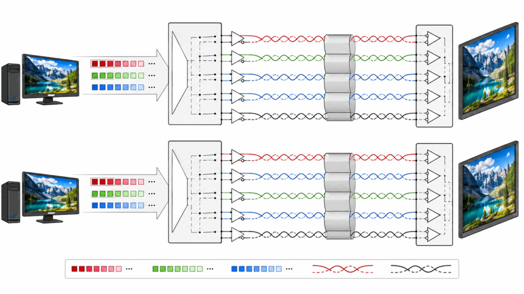
This creates an important engineering distinction: a cable may have the correct connector and differential-pair count, yet the displayed colors can still be wrong because the transmitter packs pixel bits differently from the way the panel receiver expects them.
For an RGB888 path, each red, green, and blue component contains eight bits. Some bits carry more visual weight than others. The most significant bits determine the larger steps in intensity, while the least significant bits refine smaller differences. VESA and JEIDA mappings place these bits differently across the serialized LVDS lanes.
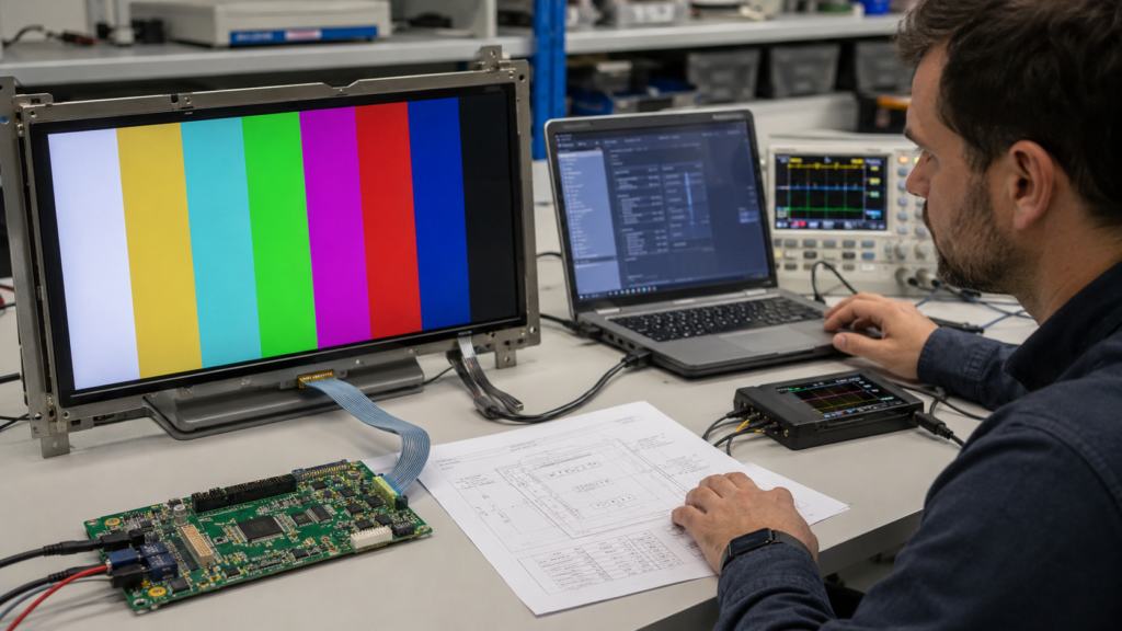
STMicroelectronics explains the practical distinction by noting that VESA groups the least significant RGB component bits on the first three data lanes, while JEIDA keeps the six most significant bits on the common three-lane portion and places the additional RGB888 bits on the fourth lane.3 This difference matters when a 24-bit transmitter and a 24-bit panel use different conventions.
| Item | What to Verify | Why It Matters |
|---|---|---|
| Color depth | RGB666 or RGB888 path | Determines the number of active color bits and commonly used data lanes |
| Data mapping | JEIDA or VESA convention stated by the panel and transmitter | Determines where significant and less-significant RGB bits are serialized |
| LVDS channel architecture | Single-channel or dual-channel implementation | Affects how pixels are divided across links; it is not the same question as VESA versus JEIDA |
| Lane order and polarity | Pair assignment, positive/negative polarity, connector pinout, and any mirror function | A mapping setting cannot correct arbitrary wiring or polarity errors |
| Pixel timing | Active area, pixel clock, sync, porches, and refresh behavior | Correct mapping does not compensate for incompatible timing |
A mapping mismatch often produces a different failure signature from missing power or incorrect timing. The panel may show a stable, correctly positioned image because the receiver is recovering the clock and control structure. However, the interpretation of color significance is wrong.
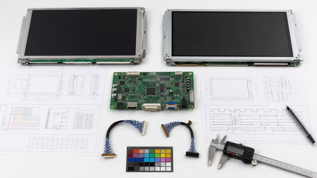
Common observations include:
These symptoms are diagnostic clues, not proof. Reversed channel order, an incorrect lane assignment, a bit-depth mismatch, a bridge-register error, or a signal-integrity problem may also corrupt color. If the display has no image, unstable synchronization, an offset active area, flicker, or intermittent startup, engineers should first review power, reset, timing, cable, signal integrity, and initialization rather than assuming a VESA/JEIDA issue.
The safest source is the complete panel specification, not a distributor summary or connector photograph. Locate the LVDS input section and identify the actual mapping diagram. The word “LVDS” alone is insufficient.
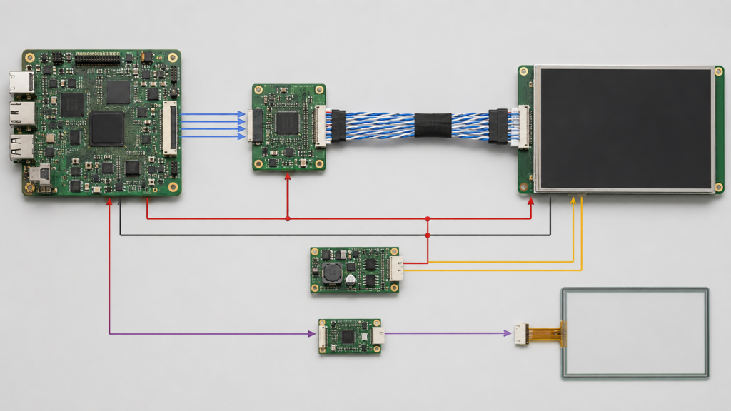
Confirm the color depth, data-pair count, clock pair, single- or dual-channel architecture, connector pinout, polarity, timing table, power rails, enable sequence, backlight requirements, and the bit mapping expected by the panel. Some documents state VESA or JEIDA directly. Others provide only a slot-by-slot diagram that must be compared with the transmitter documentation.
Do not rely only on bit labels such as R0 or R7 without reading the manufacturer’s convention. ST notes that some panel specifications label the most significant and least significant bits in ways that can create confusion.4 The diagram and explanatory notes should control the interpretation.
The host may contain a native LVDS transmitter, an RGB-to-LVDS serializer, a MIPI DSI-to-LVDS bridge, or another active conversion device. Verify whether its mapping is fixed, selected by a pin, changed through registers, or configured in firmware. Linux device-tree bindings expose mapping as an explicit property for relevant LVDS panels and codecs, which reinforces that the setting belongs in the controlled hardware/software configuration.5 For the wider system-level review, see RJY Display’s guide to matching a TFT LCD module with an Android control board.
If the source is HDMI, an active receiver or scaler must first convert the video into a panel-compatible path. A passive HDMI-to-LVDS cable cannot create the required receiver, timing, mapping, panel power, or backlight functions.
Record the panel model and revision, controller-board revision, bridge or serializer part, firmware or BSP build, cable drawing, jumper states, and relevant register or device-tree settings. Without configuration control, a corrected prototype can later fail again after a board or software revision.
Use full-intensity red, green, blue, white, and black fields together with grayscale ramps and channel gradients. A photograph may reveal that the image looks wrong, but controlled patterns make it easier to distinguish component order, bit significance, clipping, and missing shades.
Verify that the active resolution, pixel clock, synchronization, power sequence, reset, enable, and backlight behavior comply with the panel specification. Confirm the differential-pair routing and connector pinout. Do not use a mapping change to hide a wiring or timing fault.
If the transmitter supports both mappings, change only the mapping control while keeping the test pattern, timing, cable, and power configuration constant. A controlled A/B comparison is more reliable than changing several bridge registers at once.
Test the normal application UI, gradients, images, suspend/resume, cold start, warm restart, brightness transitions, and all required operating modes. A correct boot logo does not prove that every display state and software path uses the same configuration.
Add the approved mapping to the panel-control-board compatibility matrix, cable drawing, firmware manifest, device-tree source, production test procedure, and change-control record. Treat a mapping change as a compatibility change, not a cosmetic software preference.
Panel replacement projects often begin with mechanical size, resolution, connector type, brightness, and availability. Those checks are necessary but not sufficient. Two panels with similar dimensions and the same nominal LVDS interface may expect different color depth, mapping, channel architecture, timing, pinout, power, or backlight control. RJY Display’s guide to replacing a discontinued TFT LCD module explains the broader form, fit, function, lifecycle, and qualification process.
| Replacement Check | Do Not Assume | Required Evidence |
|---|---|---|
| Connector | Same connector means same pinout | Both connector tables and cable drawing |
| LVDS mapping | All 24-bit LVDS panels use one format | Panel mapping diagram and transmitter configuration |
| Timing | Same resolution means identical timing | Pixel clock, porch, sync, and refresh ranges |
| Power and backlight | The host can reuse every rail and enable signal | Power sequence, voltage/current requirements, and backlight specification |
| Software | The existing firmware will identify and drive the panel automatically | Bridge, driver, device-tree, and production-image review |
For an OEM replacement program, the appropriate goal is not to find a panel that looks similar. It is to qualify a complete controlled configuration: panel, cable, controller or bridge, firmware, power, backlight, mechanical assembly, and validation evidence.
To review an LVDS display project efficiently, provide the current panel model and datasheet, candidate panel documentation, host or controller-board information, cable drawing, required resolution and refresh behavior, bridge or serializer details, operating system or firmware version, backlight requirements, mechanical drawing, annual volume, prototype quantity, and photographs of the current image fault if troubleshooting is required.
RJY Display can evaluate available TFT LCD modules and controller-board options against a defined project requirement. The review should begin with an existing panel platform and documented compatibility needs rather than an assumption that any LVDS panel can be made interchangeable through a cable change alone. For the wider customization boundary, review the custom TFT LCD engineering guide.
Send your display, controller-board, cable, and firmware requirements for a compatibility review.
No. VESA and JEIDA mapping describe how pixel data is arranged on an LVDS display path. Connector type and pinout are separate compatibility requirements.
Yes. The panel may recover the clock and show stable geometry while colors, gradients, and intensity levels are incorrect because the RGB bits are interpreted in the wrong positions.
Only if the LVDS transmitter, bridge, or display controller supports changing the mapping through a documented hardware or software setting. Application-level color correction is not a reliable substitute for configuring the actual serializer mapping.
No. Mapping defines the arrangement of pixel bits. Single- and dual-channel architectures describe how the display data is distributed across one or two LVDS links. Both must be checked independently.
Validate mapping, color ramps, full-color fields, timing, startup, restart, suspend/resume, power sequence, backlight control, cable integrity, the complete application UI, mechanical assembly, and every required operating mode.
Share your display size, resolution, interface, brightness, touch requirement, controller board requirement, and application environment.
Continue reading related display technology guides and application references.



Talk to RJY’s engineering team for display matching, controller board review, and customization discussion.