Enfrentando um gargalo no seu Projeto de Display Incorporado?
Não deixe que a integração complexa ou problemas na cadeia de abastecimento atrasem o seu tempo de colocação no mercado. Marque uma consulta gratuita com a equipa de especialistas da RJY para apoio personalizado em design e fabrico.
Mapeamento de Dados para LCD TFT LVDS: Guia de Compatibilidade entre VESA e JEIDA
Publicado:
Leitura de 9 minutos
Atualizado:
Um LCD TFT LVDS pode ligar, travar no sinal de entrada e exibir uma imagem estável, ainda que reproduzindo as cores incorretamente. Quando a resolução e a sincronização parecem corretas, mas os gradientes estão posterizados, os tons escuros estão esmagados ou as cores parecem deslocadas de forma não natural, o problema pode estar no mapeamento de dados, e não no vidro do painel, na qualidade do cabo ou no software de aplicação.
VESA e JEIDA são convenções de mapeamento comumente referenciadas para organizar os bits de pixel RGB em um link de display LVDS. Elas não alteram o conector físico por si só e não devem ser confundidas com temporização de pixel, polaridade de lane, LVDS de canal único versus duplo, ou as características elétricas da interface. Elas definem como o transmissor e o receptor interpretam os dados de pixel serializados. Ambas as extremidades devem concordar.
Este guia explica como o mapeamento afeta um sistema LCD TFT embarcado, como distinguir um problema de mapeamento de outras falhas de compatibilidade e o que os engenheiros devem verificar antes de aprovar um painel de substituição ou uma configuração de placa controladora.
Por que o Mapeamento LVDS é um Requisito de Compatibilidade Separado
LVDS descreve um método de sinalização diferencial de baixa tensão, mas uma conexão LCD também precisa de um método acordado para transportar informações de pixel e controle. Em muitos sistemas de tela plana, um serializador converte dados RGB paralelos em um fluxo transportado por pares diferenciais, e o receptor no lado do painel reconstrói os dados de pixel.
A Texas Instruments documenta múltiplos mapeamentos RGB-para-LVDS/OpenLDI para caminhos de display de 18 e 24 bits, demonstrando que a interoperabilidade depende da atribuição dos bits de entrada corretos às saídas serializadas esperadas.1 As bindings de painel Linux tratam igualmente jeida-18, jeida-24e vesa-24 como valores distintos de mapeamento de dados, e não como nomes intercambiáveis.2
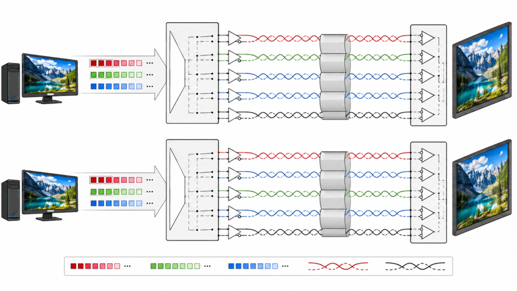
Comparação conceitual de dois mapeamentos de ordem de bits RGB através de lanes diferenciais LVDS
Isso cria uma distinção importante para a engenharia: um cabo pode ter o conector e o número de pares diferenciais corretos, mas as cores exibidas ainda podem estar erradas porque o transmissor empacota os bits de pixel de forma diferente da esperada pelo receptor do painel.
VESA vs JEIDA: O que Realmente Muda?
Para um caminho RGB888, cada componente vermelho, verde e azul contém oito bits. Alguns bits carregam mais peso visual do que outros. Os bits mais significativos determinam os maiores degraus de intensidade, enquanto os bits menos significativos refinam diferenças menores. Os mapeamentos VESA e JEIDA posicionam esses bits de forma diferente nas lanes LVDS serializadas.
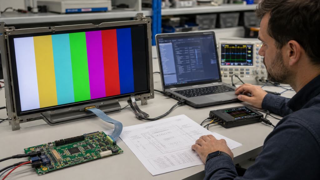
Engenheiro diagnosticando cores estáveis, mas incorretas, em um sistema LCD TFT LVDS
A STMicroelectronics explica a distinção prática ao notar que o VESA agrupa os bits menos significativos dos componentes RGB nas três primeiras lanes de dados, enquanto o JEIDA mantém os seis bits mais significativos na porção comum de três lanes e coloca os bits adicionais do RGB888 na quarta lane.3 Essa diferença é importante quando um transmissor de 24 bits e um painel de 24 bits usam convenções diferentes.
Item
O que Verificar
Por Que Isso Importa
Profundidade da cor
Caminho RGB666 ou RGB888
Determina o número de bits de cor ativos e as lanes de dados comumente usadas
Mapeamento de dados
Convenção JEIDA ou VESA declarada pelo painel e transmissor
Determina onde os bits RGB significativos e menos significativos são serializados
Arquitetura de canal LVDS
Implementação de canal único ou canal duplo
Afeta como os pixels são divididos entre os links; não é a mesma questão que VESA versus JEIDA
Ordem e polaridade das lanes
Atribuição de pares, polaridade positiva/negativa, pinagem do conector e qualquer função de espelhamento
Uma configuração de mapeamento não pode corrigir erros arbitrários de fiação ou polaridade
Temporização de pixel
Área ativa, clock de pixel, sincronismo, porches e comportamento de atualização
O mapeamento correto não compensa uma temporização incompatível
Sintomas Típicos de uma Incompatibilidade VESA/JEIDA
Uma incompatibilidade de mapeamento frequentemente produz uma assinatura de falha diferente de falta de energia ou temporização incorreta. O painel pode mostrar uma imagem estável e posicionada corretamente porque o receptor está recuperando o clock e a estrutura de controle. No entanto, a interpretação da significância da cor está errada.
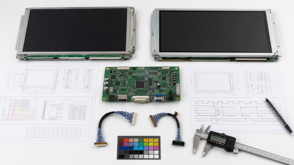
Módulos LCD TFT LVDS existentes e candidatos sob revisão de compatibilidade antes da substituição
Observações comuns incluem:
gradientes suaves tornando-se visivelmente escalonados ou posterizados;
tons escuros aparecendo muito escuros, recortados ou com matiz inesperado;
barras de cores exibindo relações de intensidade erradas;
fotografias parecendo não naturais, embora o texto e a geometria permaneçam nítidos;
um painel de substituição mostrando comportamento de cor diferente enquanto o painel original permanece correto no mesmo host.
Esses sintomas são pistas de diagnóstico, não provas. Ordem de canal invertida, atribuição de lane incorreta, incompatibilidade de profundidade de bits, erro de registro de ponte ou um problema de integridade de sinal também podem corromper as cores. Se o display não tiver imagem, sincronização instável, área ativa deslocada, cintilação ou inicialização intermitente, os engenheiros devem primeiro revisar energia, reset, temporização, cabo, integridade do sinal e inicialização, em vez de assumir um problema VESA/JEIDA.
Como Verificar o Mapeamento Antes de Conectar um Novo Painel
A fonte mais segura é a especificação completa do painel, não um resumo do distribuidor ou uma foto do conector. Localize a seção de entrada LVDS e identifique o diagrama de mapeamento real. A palavra “LVDS” sozinha é insuficiente.
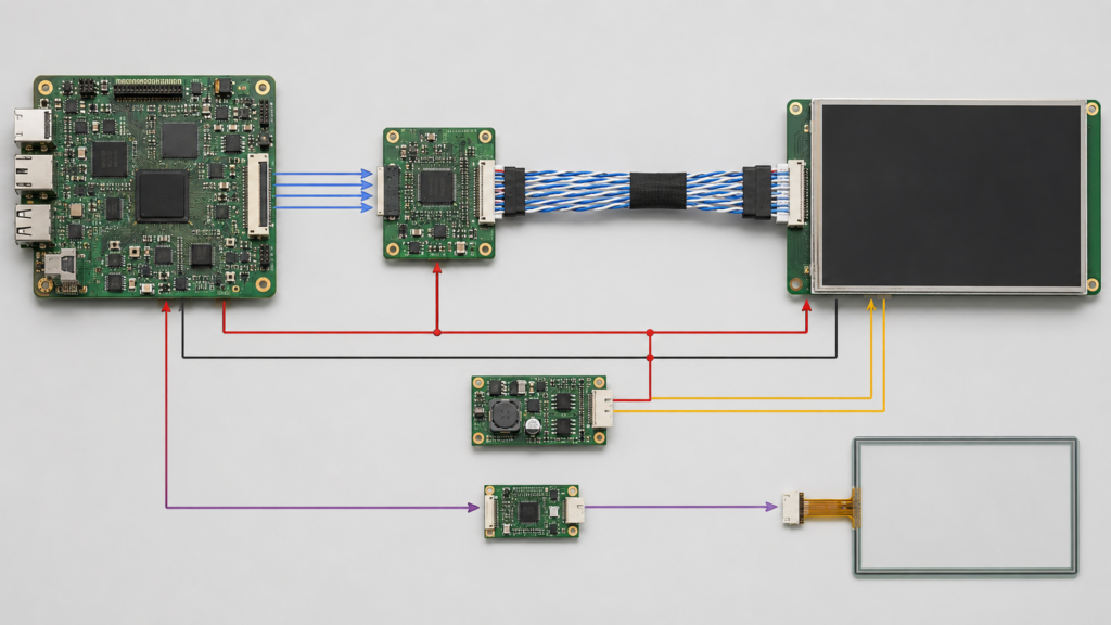
Arquitetura de display LVDS embarcado com caminhos separados de vídeo, retroiluminação, alimentação e toque
Verifique a Documentação do Painel
Confirme a profundidade de cor, contagem de pares de dados, par de clock, arquitetura de canal único ou duplo, pinagem do conector, polaridade, tabela de temporização, trilhas de alimentação, sequência de habilitação, requisitos de retroiluminação e o mapeamento de bits esperado pelo painel. Alguns documentos indicam VESA ou JEIDA diretamente. Outros fornecem apenas um diagrama slot a slot que deve ser comparado com a documentação do transmissor.
Não confie apenas em rótulos de bits como R0 ou R7 sem ler a convenção do fabricante. A ST observa que algumas especificações de painel rotulam os bits mais significativos e menos significativos de maneiras que podem criar confusão.4 O diagrama e as notas explicativas devem controlar a interpretação.
Verifique o Transmissor, Ponte ou Saída do SoC
O host pode conter um transmissor LVDS nativo, um serializador RGB-para-LVDS, uma ponte MIPI DSI-para-LVDS ou outro dispositivo de conversão ativo. Verifique se seu mapeamento é fixo, selecionado por um pino, alterado através de registros ou configurado no firmware. As bindings de device-tree do Linux expõem o mapeamento como uma propriedade explícita para painéis e codecs LVDS relevantes, o que reforça que a configuração pertence à configuração controlada de hardware/software.5 Para a revisão mais ampla em nível de sistema, consulte o guia da RJY Display para corresponder um módulo TFT LCD a uma placa de controle Android.
Se a fonte for HDMI, um receptor ou scaler ativo deve primeiro converter o vídeo em um caminho compatível com o painel. Um cabo HDMI-para-LVDS passivo não pode criar as funções necessárias de receptor, temporização, mapeamento, alimentação do painel ou retroiluminação.
Um Fluxo de Trabalho Prático para Diagnóstico de Mapeamento LVDS
1. Congele a Configuração Testada
Registre o modelo e revisão do painel, revisão da placa controladora, peça da ponte ou serializador, versão do firmware ou BSP, desenho do cabo, estados dos jumpers e configurações relevantes de registros ou device-tree. Sem controle de configuração, um protótipo corrigido pode falhar novamente após uma revisão de placa ou software.
2. Comece com Imagens de Teste Determinísticas
Use campos de vermelho, verde, azul, branco e preto em intensidade total, juntamente com rampas de cinza e gradientes de canal. Uma fotografia pode revelar que a imagem parece errada, mas padrões controlados facilitam a distinção entre ordem dos componentes, significância dos bits, recorte e tons ausentes.
3. Confirme a Temporização e a Estabilidade Elétrica
Verifique se a resolução ativa, clock de pixel, sincronismo, sequência de alimentação, reset, habilitação e comportamento da retroiluminação estão em conformidade com a especificação do painel. Confirme o roteamento dos pares diferenciais e a pinagem do conector. Não use uma alteração de mapeamento para ocultar uma falha de fiação ou temporização.
4. Compare os Dois Estados de Mapeamento Deliberadamente
Se o transmissor suportar ambos os mapeamentos, altere apenas o controle de mapeamento, mantendo constantes o padrão de teste, o timing, o cabo e a configuração de energia. Uma comparação controlada A/B é mais confiável do que alterar vários registros da ponte de uma só vez.
5. Valide Mais do Que a Tela de Inicialização
Teste a interface de usuário normal do aplicativo, gradientes, imagens, suspensão/retomada, inicialização a frio, reinicialização a quente, transições de brilho e todos os modos de operação necessários. Um logotipo de inicialização correto não prova que todos os estados de exibição e caminhos de software usam a mesma configuração.
6. Bloqueie o Mapeamento na Documentação de Produção
Adicione o mapeamento aprovado à matriz de compatibilidade da placa de controle do painel, ao desenho do cabo, ao manifesto do firmware, à fonte da árvore de dispositivos, ao procedimento de teste de produção e ao registro de controle de alterações. Trate uma alteração de mapeamento como uma alteração de compatibilidade, não como uma preferência cosmética de software.
Por que o Mapeamento é Importante Durante a Substituição de um Painel LVDS
Projetos de substituição de painéis geralmente começam com tamanho mecânico, resolução, tipo de conector, brilho e disponibilidade. Essas verificações são necessárias, mas não suficientes. Dois painéis com dimensões semelhantes e a mesma interface LVDS nominal podem esperar profundidade de cor, mapeamento, arquitetura de canal, timing, pinagem, energia ou controle de retroiluminação diferentes. O guia da RJY Display para substituir um módulo TFT LCD descontinuado explica o processo mais amplo de forma, ajuste, função, ciclo de vida e qualificação.
Verificação de Substituição
Não Presuma
Evidência Necessária
Conector
Mesmo conector significa mesma pinagem
Tabelas de conectores e desenho do cabo
Mapeamento LVDS
Todos os painéis LVDS de 24 bits usam um formato
Diagrama de mapeamento do painel e configuração do transmissor
Tempo
Mesma resolução significa timing idêntico
Clock de pixel, pórtico, sincronismo e faixas de atualização
Energia e retroiluminação
O host pode reutilizar cada trilha e sinal de habilitação
Sequência de energia, requisitos de tensão/corrente e especificação da retroiluminação
Software
O firmware existente identificará e acionará o painel automaticamente
Revisão da ponte, driver, árvore de dispositivos e imagem de produção
Para um programa de substituição OEM, o objetivo apropriado não é encontrar um painel que pareça semelhante. É qualificar uma configuração controlada completa: painel, cabo, controlador ou ponte, firmware, energia, retroiluminação, montagem mecânica e evidência de validação.
Informações a Fornecer para uma Revisão de Compatibilidade LVDS
Para revisar um projeto de display LVDS de forma eficiente, forneça o modelo e datasheet do painel atual, documentação do painel candidato, informações do host ou placa controladora, desenho do cabo, resolução e comportamento de atualização necessários, detalhes da ponte ou serializador, versão do sistema operacional ou firmware, requisitos de retroiluminação, desenho mecânico, volume anual, quantidade de protótipos e fotografias do defeito de imagem atual, se for necessária solução de problemas.
A RJY Display pode avaliar módulos TFT LCD disponíveis e opções de placa controladora em relação a um requisito de projeto definido. A revisão deve começar com uma plataforma de painel existente e necessidades de compatibilidade documentadas, em vez da suposição de que qualquer painel LVDS pode ser intercambiável apenas por meio de uma alteração de cabo. Para o limite de personalização mais amplo, revise o guia de engenharia de TFT LCD personalizado.
Os conectores físicos VESA e JEIDA são diferentes?
Não. O mapeamento VESA e JEIDA descreve como os dados de pixel são organizados em um caminho de display LVDS. O tipo de conector e a pinagem são requisitos de compatibilidade separados.
A imagem pode permanecer estável quando o mapeamento LVDS está errado?
Sim. O painel pode recuperar o clock e mostrar geometria estável enquanto as cores, gradientes e níveis de intensidade estão incorretos porque os bits RGB são interpretados nas posições erradas.
O software pode corrigir uma incompatibilidade entre VESA e JEIDA?
Somente se o transmissor LVDS, ponte ou controlador de display suportar a alteração do mapeamento por meio de uma configuração documentada de hardware ou software. A correção de cores em nível de aplicativo não é um substituto confiável para configurar o mapeamento real do serializador.
VESA versus JEIDA é o mesmo que LVDS de canal único versus canal duplo?
Não. O mapeamento define a disposição dos bits de pixel. As arquiteturas de canal único e duplo descrevem como os dados de exibição são distribuídos em um ou dois links LVDS. Ambos devem ser verificados de forma independente.
O que deve ser testado após a troca de um painel LVDS?
Valide o mapeamento, rampas de cores, campos de cores completas, timing, inicialização, reinicialização, suspensão/retomada, sequência de energia, controle de retroiluminação, integridade do cabo, interface de usuário completa do aplicativo, montagem mecânica e todos os modos de operação necessários.