Facing a bottleneck in your Embedded Display Project?
Don’t let complex integration or supply chain issues slow your time-to-market. Book a free consultation with the RJY expert team for tailored design and manufacturing support.

Two TFT LCD modules can have the same active resolution and use the same interface family, yet require different controller-board settings. One panel may operate correctly while the other remains black, shifts the image, crops an edge, repeats part of the frame or starts only some of the time.
The missing information is often the complete display timing. A resolution such as 800 × 480 describes the visible pixel area. It does not describe the horizontal and vertical blanking intervals, synchronization pulse widths, signal polarity, sampling edge or required LCD pixel clock. Those parameters tell the panel when each active line and frame begins and ends.
This guide explains how pixel clock, porches, synchronization signals and Data Enable affect TFT LCD compatibility. It also provides a practical process for comparing a panel with a controller board without treating resolution or connector type as proof of compatibility.
A display controller sends image data in a repeated sequence. It transmits one line at a time and combines the lines into a complete frame. The active image occupies only part of that sequence. The controller also produces intervals that separate one line from the next and one frame from the next.
For a parallel RGB panel, the host can expose this structure through Pixel Clock, horizontal synchronization, vertical synchronization and Data Enable signals. Other interfaces package or serialize the information differently, but the panel still needs a valid image cadence and a supported native mode.
The active area contains the pixels that appear on the screen. An 800 × 480 panel has 800 active pixel positions in each line and 480 active lines in each frame. These values are often called Hactive and Vactive.
Active resolution is easy to compare, which is why product listings emphasize it. However, it is only one part of the mode.
Each line also contains a horizontal front porch, an HSYNC interval and a horizontal back porch. Each frame contains corresponding vertical intervals. These non-active periods form the horizontal and vertical blanking regions.
The controller must therefore generate more pixel periods than the number of visible pixels. The complete line length is the horizontal total. The complete frame height is the vertical total.
The panel driver must know which transmitted values belong to the visible image. It also needs a consistent boundary between lines and frames. Depending on the panel mode, it uses HSYNC, VSYNC, Data Enable or a combination of these signals.
Incorrect boundaries can make the driver start a line too early, accept inactive data as pixels or lose frame alignment. A display can therefore receive valid color data but place it in the wrong part of the image.
| Parameter | Meaning | Why it matters |
|---|---|---|
| Hactive | Visible pixels in each line | Sets the active image width |
| HFP | Horizontal front porch | Separates active data from the horizontal sync interval |
| HSYNC | Horizontal sync pulse width | Marks or supports the line boundary |
| HBP | Horizontal back porch | Separates the sync interval from the next active line |
| Vactive | Visible lines in each frame | Sets the active image height |
| VFP | Vertical front porch | Separates the active frame from vertical sync |
| VSYNC | Vertical sync pulse width | Marks or supports the frame boundary |
| VBP | Vertical back porch | Separates vertical sync from the next active frame |
| DE | Data Enable | Identifies periods that contain active pixels |
| PCLK | Pixel Clock | Controls the rate at which pixel periods advance |
Panel datasheets do not always use the same labels. They may describe porches as margins or list only total blanking. Follow the definitions in the exact panel datasheet.
The LCD pixel clock sets the rate of the pixel periods in a video timing stream. For a typical parallel RGB interface, the controller presents pixel data and the panel samples that data on the specified clock edge. One clock period normally advances the transfer by one pixel position, including positions inside blanking intervals.
The required clock depends on the horizontal total, vertical total and refresh rate. It does not depend on active resolution alone.
Refresh rate states how many complete frames occur each second. Pixel clock states how many pixel periods occur each second. A 60 Hz frame rate does not imply a 60 MHz pixel clock. The clock value also depends on how many total periods make up each frame.
The basic relationships are:
Horizontal Total = Hactive + HFP + HSYNC + HBP

Vertical Total = Vactive + VFP + VSYNC + VBP

Pixel Clock = Horizontal Total × Vertical Total × Refresh Rate
This formula is a useful check, but the panel datasheet remains authoritative. The driver IC may accept only a stated clock range or a limited set of timing combinations.
Consider an illustrative 800 × 480 timing. The following values are examples for calculation only. They are not a specification for an RJY product or a universal 800 × 480 mode.
| Item | Illustrative value |
|---|---|
| Hactive | 800 pixel periods |
| Combined horizontal blanking | 256 pixel periods |
| Horizontal total | 1,056 pixel periods |
| Vactive | 480 lines |
| Combined vertical blanking | 45 lines |
| Vertical total | 525 lines |
| Refresh rate | 60 frames per second |
Pixel Clock = 1,056 × 525 × 60
            = 33,264,000 Hz
            ≈ 33.264 MHz
If an engineer calculates only the active pixels, the result is:
800 × 480 × 60 = 23.04 MHzThat result omits every blanking period. In this example, it would understate the required clock by more than 10 MHz. This difference explains why resolution and frame rate alone cannot define a panel timing.
Many datasheets provide typical, minimum and maximum values. Values inside each individual range do not always create a valid combined mode. The total clock must also stay within its supported range.
Start from the recommended typical mode. Change a porch, clock or refresh rate only when the panel documentation and host design allow the change, then verify the result on the complete system.
A porch is an inactive interval beside the active video region. The terms came from raster-display timing, but they still describe the blanking structure used by modern digital panel interfaces.
A line commonly contains active pixel data, a horizontal front porch, an HSYNC pulse and a horizontal back porch. The exact order shown in a datasheet can depend on the reference point used in the diagram. What matters is that the host reproduces the required interval sizes and polarity.
The front porch separates the end of active data from the sync event. The back porch separates that event from the start of the next active line. The HSYNC width defines the duration of the synchronization pulse when the selected mode uses it.
Vertical timing follows the same concept, but its units are lines rather than pixel clocks. The sequence includes active lines, a vertical front porch, a VSYNC interval and a vertical back porch.
Two modes can have the same horizontal total but assign different values to HFP, HSYNC and HBP. They do not necessarily behave the same. The panel may use a specific edge or interval to reset an internal line counter or prepare the next active region.
Do not redistribute porch values merely to preserve the total. Confirm the permitted values from the panel timing table. If the datasheet lists only total blanking, request the detailed timing or a validated initialization reference from the panel supplier.
HSYNC identifies horizontal timing boundaries. VSYNC identifies vertical timing boundaries. Data Enable indicates when the data bus contains active image pixels. Different panels use these signals in different modes.
In a synchronization-based mode, the panel uses HSYNC and VSYNC to identify line and frame timing. The controller must generate the pulse widths, porches and active periods that the panel expects.
In SYNC-DE mode, the panel receives synchronization signals and Data Enable. DE qualifies the active image region while HSYNC and VSYNC preserve line and frame structure.
Some panels support a mode in which Data Enable defines the active region and the panel does not use external HSYNC and VSYNC inputs. This does not remove the need for correct totals and blanking. The width of DE, the gap between active lines and the gap between active frames still form a timing pattern.
A host controller can output several signals at once, but that does not prove that every connected panel can use the same configuration. Select the mode documented for the panel and connect only the signals required by that design.
Frequency and pulse width are not enough. A panel also expects each control signal to be active at a defined logic level. HSYNC, VSYNC and DE can be active high or active low. The panel may sample pixel data on the rising or falling edge of Pixel Clock.
If the host uses the wrong sync polarity, the panel can interpret inactive time as the sync pulse or fail to recognize the intended event. Incorrect DE polarity can mark blanking as active data and active data as blanking. The result may be a black display, an unstable frame, a shifted image or an image that appears only under some conditions.
The data bus must remain stable for a specified period before and after the sampling edge. These intervals are the setup and hold times. Long PCB routes, unsuitable level shifting, connector loss, clock skew and incorrect output-edge settings can reduce the available margin.
For higher-speed designs, a correct average clock frequency does not prove adequate signal quality. Engineers must also review waveform integrity and timing at the panel input.
Resolution defines the active pixel matrix. It does not standardize the electronics around that matrix.
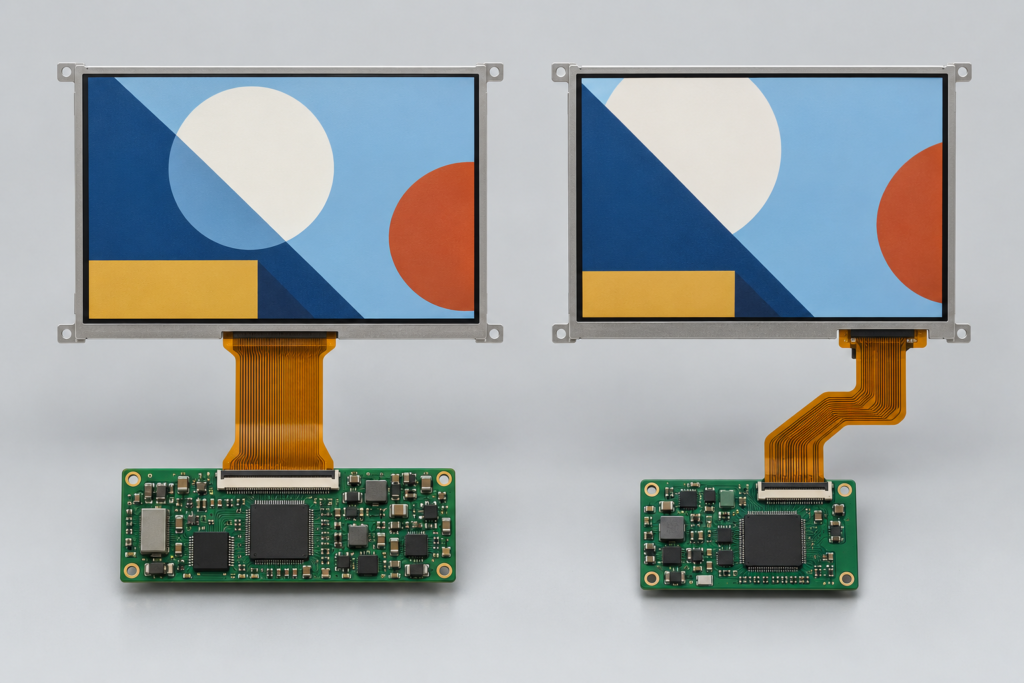
Two modules can use different timing-controller or source-driver designs. Each driver can have its own accepted blanking range, polarity, sampling edge and initialization sequence. A replacement panel may therefore need a new controller-board configuration even when the active pixels match.
Gate-driver integration, source-driver arrangement and internal timing generation can change the required input mode. An integrated timing controller can accept a different range from a module that depends more directly on external timing.
A host may generate a common 60 Hz mode, but the panel datasheet can specify another typical rate or a limited allowable range. Changing the blanking while retaining 60 Hz also changes the required Pixel Clock.
One RGB panel may use SYNC-DE mode while another uses DE-only mode. The FPC can carry similar data lines, yet the controller and pin definition still need different treatment.
Even identical display timing does not prove full compatibility. Check the connector and pin definition, power rails, reset sequence, backlight circuit, touch interface, image orientation, driver support and mechanical fit. Timing is one system layer, not a substitute for the rest of the review.
Parallel RGB makes timing easy to observe. Separate conductors commonly carry red, green and blue data together with Pixel Clock, DE and synchronization signals. The display controller produces the raster timing directly.
This visibility does not make the interface universal. Data width, color ordering, voltage, polarity, sampling edge and timing must still match.
An LVDS transmitter serializes pixel and control information into differential pairs. The panel receiver reconstructs the data. The system still needs a valid native mode, correct LVDS mapping, suitable channel count, supported bit depth and correct clock relationship.
Pixel Clock is related to the transported pixel rate, but it is not the same value as the serial bit rate on an LVDS pair. Serialization ratio and link architecture affect the physical data rate.
MIPI DSI video mode transports a video stream in packets over one or more high-speed data lanes. Active video and blanking requirements affect the data that must cross the link. Lane count, pixel format, operating mode, overhead and D-PHY settings determine whether the host has enough capacity.
The familiar RGB timing values can still appear in the host configuration, but the DSI lane clock is not simply equal to Pixel Clock. Use the SoC, bridge and panel documentation to calculate and validate the link.
Command-mode panels can receive updates through display commands and may use internal frame memory. Their transfer behavior differs from a continuous parallel RGB stream. Do not apply a video-mode calculation without confirming how the selected panel and host implement command mode.
eDP carries standardized packetized display data, while HDMI often appears as an input to a controller board rather than as the native interface of a bare LCD module. A board must still output a panel-supported mode on the internal display side.
An HDMI source showing the correct resolution does not prove that an HDMI-to-MIPI or HDMI-to-LVDS board can drive a given panel. The active conversion depends on the bridge, output interface, panel timing, firmware and physical connection.
Larger blanking intervals increase the horizontal or vertical total. At the same refresh rate, this raises Pixel Clock. More pixel periods per second also increase the rate at which the display pipeline must move data.
The impact extends beyond the panel connector:
A simple framebuffer bandwidth estimate often starts with active pixels, bytes per pixel and frames per second. Real system demand can be higher because of graphics layers, memory bursts, alignment, scaling and other access. Link bandwidth calculations also include encoding or packet overhead that is specific to the interface.
Do not treat one Pixel Clock formula as a complete system bandwidth model. Use it to establish the raster rate, then check each controller, bridge, memory and physical-link limit.
| Symptom | Timing-related checks | Other checks |
|---|---|---|
| Black screen | Pixel Clock, DE, sync mode, polarity | Power, reset, initialization, data path, backlight |
| White screen with backlight | Valid active video and timing | Panel initialization, pinout, interface and controller support |
| Horizontal image shift | HFP, HBP, HSYNC and active width | Data mapping and cropping settings |
| Vertical image shift | VFP, VBP, VSYNC and active height | Rotation, scaling and framebuffer configuration |
| Cropped edge | Active area and total timing | Scaling, OSD or source-mode configuration |
| Repeated or wrapped region | Line or frame boundary values | Framebuffer stride and bridge configuration |
| Flicker | Clock stability, refresh rate, sync and DE | Power noise, backlight PWM, cable and signal integrity |
| Intermittent startup | Timing enable and clock startup | Power sequence, reset, firmware and temperature |
These symptoms are clues, not proof. For example, flicker can come from an unstable Pixel Clock, but it can also come from the LED driver or a poor connector. Diagnose the display as a system.
Record the LCD model and revision, driver IC when available, controller-board model, bridge IC, connector and PCB revision. Compatibility cannot be confirmed from screen size and resolution alone.
Create a table for active resolution, total resolution, porches, sync widths, refresh rate, Pixel Clock, polarity and sampling edge. Compare it with the modes that the controller or firmware can generate.
For LVDS, include mapping, channel count and bit depth. For MIPI DSI, include lane count, pixel format, video or command mode, lane-rate limits and initialization commands. For RGB, include data width and voltage.
A processor may calculate its display clock from a parent clock and integer or fractional divider. The exact requested value may not be available. Confirm the actual generated clock and ensure that the resulting frame rate remains inside the panel limits.
The board support package, device tree, bootloader or controller firmware must describe the correct mode. A hardware-capable board can still fail if the software loads a default timing for another panel.
Correct video timing cannot repair a wrong supply, reset pulse, initialization sequence or LED-driver mismatch. Keep these checks in the same validation plan, but do not confuse them with raster timing.
Test cold power-up, warm restart, signal reconnect, sleep, wake and controlled power-down. Observe whether the clock and active video start only after the panel is ready and whether the backlight exposes an invalid frame.
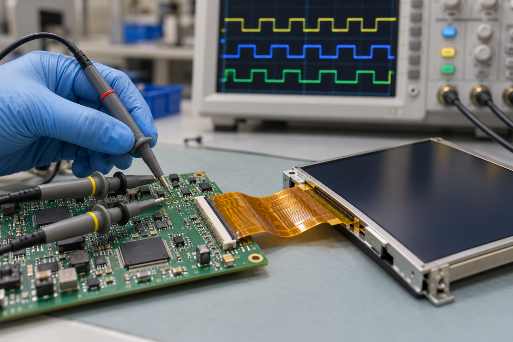
On accessible parallel signals, an oscilloscope can measure Pixel Clock frequency, HSYNC rate, VSYNC rate, DE width, polarity and startup order. From the measured HSYNC and VSYNC rates, engineers can check whether the actual line and frame cadence agrees with the intended mode.
Use probes and bandwidth appropriate for the signal. Poor probing can distort an edge or add enough loading to change behavior. Differential high-speed links require suitable differential measurement equipment and methods.
A logic analyzer can help with lower-speed control signals, GPIO sequencing, SPI initialization or I²C configuration. It is not automatically suitable for capturing every MIPI, LVDS or eDP physical-layer signal. Use protocol-specific equipment when the link speed and signaling method require it.
A measurement shows what the board generates, not what the panel accepts. Compare it with the approved specification.
A typical embedded display configuration can include:
Linux display drivers and device trees often store mode parameters as separate clock, active-area, margin, sync-length and polarity values. An Android-based board can use the same kernel-level configuration concepts even though the user interface runs on Android.
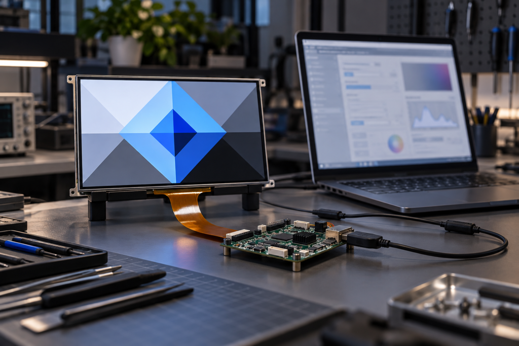
Firmware adaptation is therefore a real part of panel matching. It should be planned with the hardware review rather than treated as a final software setting after the board is complete.
RJY Display can review display timing as part of a project-specific LCD and controller-board configuration. Depending on the selected panel and host platform, the scope can include:
This is a compatibility process, not a universal board claim. The result depends on the exact LCD, controller hardware, firmware, operating system and application environment. An active HDMI-to-MIPI or HDMI-to-LVDS path must be designed for the selected panel; it is not a passive cable conversion.
Send the following information where available:
If the current system already works with another panel, include that panel’s datasheet and approved configuration. A side-by-side comparison often shows whether the difference lies in timing, pinout, interface mode, power or software.
LCD pixel clock connects resolution, blanking and refresh rate, but it is not the only compatibility parameter. Engineers must also preserve the required porches, sync widths, Data Enable behavior, polarity and sampling edge. The chosen interface and firmware then need to carry or generate that mode correctly.
This is why two same-resolution panels can produce different results on the same board. Treat the panel timing table as part of the hardware specification, not as an optional software detail.
For related engineering guidance, review LCD display interfaces, compare MIPI and LVDS for industrial LCDs, or read the LVDS data-mapping guide. If you are matching a panel to a host platform, see how to match a TFT LCD with an Android board. For a project review, submit your LCD timing and controller-board information.
Pixel Clock is the rate at which pixel periods advance in a display timing stream. It includes active pixels and the pixel periods used by horizontal and vertical blanking.
Add the active width, horizontal porches and HSYNC width to obtain the horizontal total. Add the active height, vertical porches and VSYNC width to obtain the vertical total. Multiply both totals by the refresh rate. Then compare the result with the panel’s specified clock range.
No. Refresh rate is the number of complete frames per second. Pixel Clock is the number of pixel periods per second. The totals for each line and frame connect the two values.
They can use different driver ICs, blanking intervals, synchronization modes, clock ranges, signal polarities and initialization requirements. Resolution describes only the active pixel matrix.
Do not assume so. A panel can require specific front porch, sync width and back porch ranges even when the total is unchanged. Use the exact datasheet limits and validate the complete system.
The panel may fail to recognize line or frame boundaries. Possible results include a black screen, image shift, unstable display or intermittent operation. These symptoms can also have other causes.
Yes. These interfaces transport display data differently from parallel RGB, but the host, bridge and panel still need a supported native mode. Link mapping, lane configuration, throughput and firmware must also match.
No. A review also needs the LCD model, interface, pin definition, timing, driver IC when available, power, backlight, touch, firmware, operating system and application requirements.
Share your display size, resolution, interface, brightness, touch requirement, controller board requirement, and application environment.
Continue reading related display technology guides and application references.
Talk to RJY’s engineering team for display matching, controller board review, and customization discussion.