Stehen Sie bei Ihrem Embedded-Display-Projekt vor einer Herausforderung?
Lassen Sie nicht komplexe Integration oder Lieferkettenprobleme Ihre Markteinführung verzögern. Vereinbaren Sie eine kostenlose Beratung mit dem RJY-Expertenteam für maßgeschneiderte Design- und Fertigungsunterstützung.
LCD-Pixel-Takt- und Timing-Leitfaden: Warum TFT-Displays mit gleicher Auflösung nicht immer kompatibel sind
Veröffentlicht:
18 Min. Lesezeit
Aktualisiert:
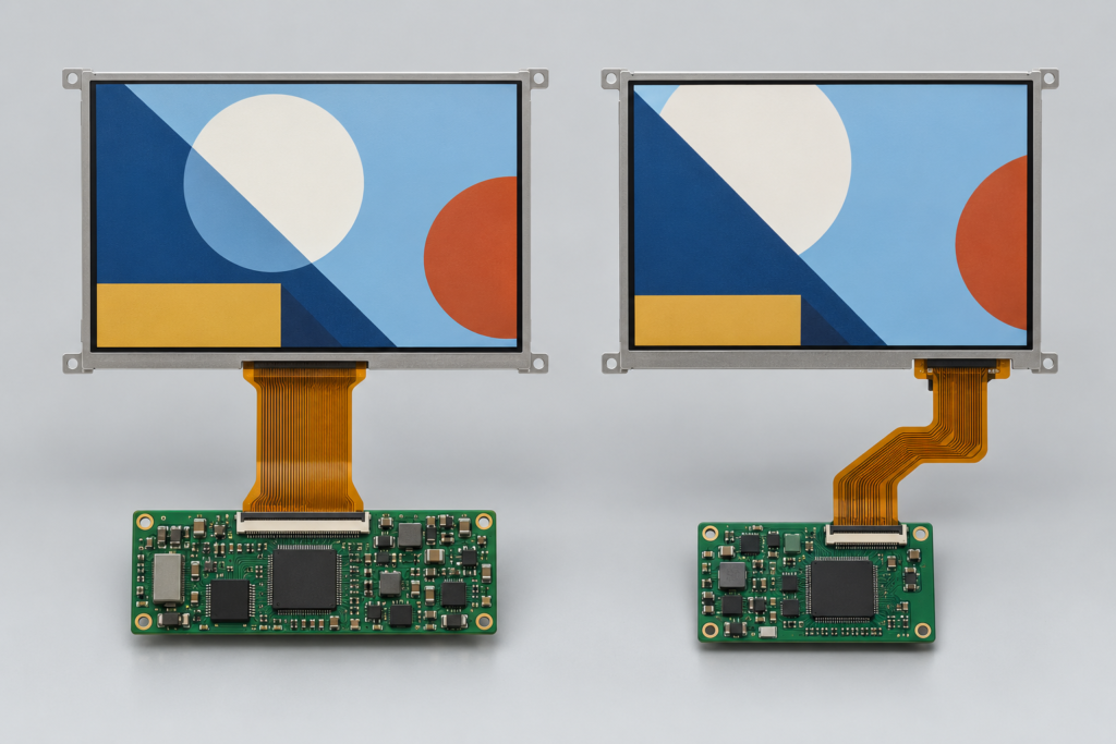
Zwei TFT-LCD-Module können dieselbe aktive Auflösung haben und dieselbe Schnittstellenfamilie verwenden und dennoch unterschiedliche Einstellungen am Controller-Board erfordern. Ein Panel kann korrekt arbeiten, während das andere schwarz bleibt, das Bild verschiebt, einen Rand abschneidet, einen Teil des Frames wiederholt oder nur zeitweise startet.
Die fehlende Information ist häufig das vollständige Display-Timing. Eine Auflösung wie 800 × 480 beschreibt die sichtbare Pixelfläche. Sie beschreibt nicht die horizontalen und vertikalen Blanking-Intervalle, die Synchronisationspulsbreiten, die Signalpolarität, die Abtastflanke oder den erforderlichen LCD-Pixel-Takt. Diese Parameter teilen dem Panel mit, wann jede aktive Zeile und jeder Frame beginnt und endet.
Dieser Leitfaden erklärt, wie Pixel-Takt, Porches, Synchronisationssignale und Data Enable die TFT-LCD-Kompatibilität beeinflussen. Er bietet außerdem einen praktischen Prozess zum Vergleich eines Panels mit einem Controller-Board, ohne Auflösung oder Steckertyp als Beweis für Kompatibilität zu behandeln.
Was ist LCD-Display-Timing?
Ein Display-Controller sendet Bilddaten in einer wiederholten Sequenz. Er überträgt jeweils eine Zeile und kombiniert die Zeilen zu einem vollständigen Frame. Das aktive Bild belegt nur einen Teil dieser Sequenz. Der Controller erzeugt außerdem Intervalle, die eine Zeile von der nächsten und einen Frame vom nächsten trennen.
Bei einem Parallel-RGB-Panel kann der Host diese Struktur über Pixel Clock, horizontale Synchronisation, vertikale Synchronisation und Data Enable bereitstellen. Andere Schnittstellen verpacken oder serialisieren die Informationen anders, aber das Panel benötigt weiterhin eine gültige Bildfolge und einen unterstützten nativen Modus.
Aktiver Bildbereich
Der aktive Bereich enthält die Pixel, die auf dem Bildschirm erscheinen. Ein 800 × 480 Panel hat 800 aktive Pixelpositionen in jeder Zeile und 480 aktive Zeilen in jedem Frame. Diese Werte werden häufig als Hactive und Vactive bezeichnet.
Die aktive Auflösung ist leicht zu vergleichen, weshalb Produktlistings sie hervorheben. Sie ist jedoch nur ein Teil des Modus.
Gesamter Timing-Bereich
Jede Zeile enthält außerdem einen horizontalen Front Porch, ein HSYNC-Intervall und einen horizontalen Back Porch. Jeder Frame enthält entsprechende vertikale Intervalle. Diese nicht aktiven Perioden bilden die horizontalen und vertikalen Blanking-Bereiche.
Der Controller muss daher mehr Pixelperioden erzeugen als die Anzahl der sichtbaren Pixel. Die vollständige Zeilenlänge ist das horizontale Total. Die vollständige Frame-Höhe ist das vertikale Total.
Warum das Panel Timing-Grenzen benötigt
Der Panel-Treiber muss wissen, welche übertragenen Werte zum sichtbaren Bild gehören. Er benötigt außerdem eine konsistente Grenze zwischen Zeilen und Frames. Je nach Panel-Modus verwendet er HSYNC, VSYNC, Data Enable oder eine Kombination dieser Signale.
Falsche Grenzen können dazu führen, dass der Treiber eine Zeile zu früh startet, inaktive Daten als Pixel akzeptiert oder die Frame-Ausrichtung verliert. Ein Display kann daher gültige Farbdaten empfangen, sie aber im falschen Teil des Bildes platzieren.
Wichtige TFT-LCD-Timing-Parameter
Parameter
Bedeutung
Warum es wichtig ist
Hactive
Sichtbare Pixel in jeder Zeile
Legt die aktive Bildbreite fest
HFP
Horizontaler Front Porch
Trennt aktive Daten vom horizontalen Sync-Intervall
HSYNC
Horizontale Sync-Pulsbreite
Markiert oder unterstützt die Zeilengrenze
HBP
Horizontaler Back Porch
Trennt das Sync-Intervall von der nächsten aktiven Zeile
Vactive
Sichtbare Zeilen in jedem Frame
Legt die aktive Bildhöhe fest
VFP
Vertikale vordere Austastlücke
Trennt das aktive Bild vom vertikalen Sync
VSYNC
Pulsbreite des vertikalen Sync
Markiert oder unterstützt die Bildgrenze
VBP
Vertikale hintere Austastlücke
Trennt den vertikalen Sync vom nächsten aktiven Bild
DE
Data Enable
Kennzeichnet Zeiträume, die aktive Pixel enthalten
PCLK
Pixel Clock
Steuert die Rate, mit der Pixelperioden fortgeschritten werden
Panel-Datenblätter verwenden nicht immer dieselben Bezeichnungen. Sie können Austastlücken als Ränder beschreiben oder nur die gesamte Austastung angeben. Befolgen Sie die Definitionen im exakten Panel-Datenblatt.
Was ist der LCD-Pixel-Takt?
Die LCD-Pixel-Clock legt die Rate der Pixelperioden in einem Video-Timing-Stream fest. Bei einer typischen parallelen RGB-Schnittstelle stellt der Controller Pixeldaten bereit, und das Panel tastet diese Daten an der angegebenen Clock-Flanke ab. Eine Clock-Periode verschiebt den Transfer normalerweise um eine Pixelposition, einschließlich Positionen innerhalb von Austastintervallen.
Die erforderliche Clock hängt von der horizontalen Gesamtsumme, der vertikalen Gesamtsumme und der Bildwiederholrate ab. Sie hängt nicht allein von der aktiven Auflösung ab.
Pixel Clock ist nicht die Bildwiederholrate
Die Bildwiederholrate gibt an, wie viele vollständige Bilder pro Sekunde auftreten. Die Pixel Clock gibt an, wie viele Pixelperioden pro Sekunde auftreten. Eine Bildrate von 60 Hz impliziert keine Pixel Clock von 60 MHz. Der Clock-Wert hängt auch davon ab, wie viele Gesamtperioden jedes Bild umfassen.
Die grundlegenden Beziehungen sind:
Horizontal Total = Hactive + HFP + HSYNC + HBP
Diese Formel ist eine nützliche Überprüfung, aber das Panel-Datenblatt bleibt maßgeblich. Der Treiber-IC akzeptiert möglicherweise nur einen angegebenen Clock-Bereich oder eine begrenzte Gruppe von Timing-Kombinationen.
Eine praktische Pixel-Takt-Berechnung
Betrachten Sie ein veranschaulichendes 800 × 480-Timing. Die folgenden Werte sind nur Beispiele zur Berechnung. Sie sind keine Spezifikation für ein RJY-Produkt oder einen universellen 800 × 480-Modus.
Artikel
Veranschaulichender Wert
Hactive
800 Pixelperioden
Kombinierte horizontale Austastung
256 Pixelperioden
Horizontale Gesamtsumme
1.056 Pixelperioden
Vactive
480 Zeilen
Kombinierte vertikale Austastung
45 Zeilen
Vertikale Gesamtsumme
525 Zeilen
Bildwiederholfrequenz
60 Bilder pro Sekunde
Pixel Clock = 1.056 × 525 × 60
Wenn ein Ingenieur nur die aktiven Pixel berechnet, lautet das Ergebnis:
800 × 480 × 60 = 23,04 MHz
Dieses Ergebnis lässt jede Austastperiode weg. In diesem Beispiel würde es die erforderliche Clock um mehr als 10 MHz unterschätzen. Dieser Unterschied erklärt, warum Auflösung und Bildrate allein kein Panel-Timing definieren können.
Typische, minimale und maximale Werte
Viele Datenblätter geben typische, minimale und maximale Werte an. Werte innerhalb jedes einzelnen Bereichs erzeugen nicht immer einen gültigen kombinierten Modus. Die Gesamt-Clock muss auch innerhalb ihres unterstützten Bereichs bleiben.
Beginnen Sie mit dem empfohlenen typischen Modus. Ändern Sie eine Austastlücke, die Clock oder die Bildwiederholrate nur, wenn die Panel-Dokumentation und das Host-Design die Änderung zulassen, und verifizieren Sie das Ergebnis anschließend im vollständigen System.
Front Porch, Back Porch und Sync-Breite
Eine Austastlücke ist ein inaktives Intervall neben dem aktiven Videobereich. Die Begriffe stammen aus dem Timing von Rasteranzeigen, beschreiben aber weiterhin die Blanking-Struktur, die von modernen digitalen Panel-Schnittstellen verwendet wird.
Horizontale Timing-Sequenz
Eine Zeile enthält üblicherweise aktive Pixeldaten, eine horizontale vordere Austastlücke, einen HSYNC-Puls und eine horizontale hintere Austastlücke. Die genaue Reihenfolge, die in einem Datenblatt dargestellt wird, kann vom Referenzpunkt im Diagramm abhängen. Entscheidend ist, dass der Host die erforderlichen Intervallgrößen und Polaritäten reproduziert.
Die vordere Austastlücke trennt das Ende der aktiven Daten vom Sync-Ereignis. Die hintere Austastlücke trennt dieses Ereignis vom Beginn der nächsten aktiven Zeile. Die HSYNC-Breite definiert die Dauer des Synchronisationspulses, wenn der ausgewählte Modus ihn verwendet.
Vertikale Timing-Sequenz
Das vertikale Timing folgt demselben Konzept, aber seine Einheiten sind Zeilen statt Pixel-Clocks. Die Sequenz umfasst aktive Zeilen, eine vertikale vordere Austastlücke, ein VSYNC-Intervall und eine vertikale hintere Austastlücke.
Warum Austastlückenwerte nicht frei austauschbar sind
Zwei Modi können dieselbe horizontale Gesamtsumme haben, aber unterschiedliche Werte für HFP, HSYNC und HBP zuweisen. Sie verhalten sich nicht zwangsläufig gleich. Das Panel verwendet möglicherweise eine bestimmte Flanke oder ein bestimmtes Intervall, um einen internen Zeilenzähler zurückzusetzen oder den nächsten aktiven Bereich vorzubereiten.
Verteilen Sie Austastlückenwerte nicht allein neu, um die Gesamtsumme beizubehalten. Bestätigen Sie die zulässigen Werte aus der Panel-Timing-Tabelle. Wenn das Datenblatt nur die gesamte Austastung angibt, fordern Sie das detaillierte Timing oder eine validierte Initialisierungsreferenz vom Panel-Lieferanten an.
HSYNC, VSYNC und Data Enable
HSYNC kennzeichnet horizontale Timing-Grenzen. VSYNC kennzeichnet vertikale Timing-Grenzen. Data Enable zeigt an, wann der Datenbus aktive Bildpixel enthält. Verschiedene Panels verwenden diese Signale in unterschiedlichen Modi.
SYNC mode
In a synchronization-based mode, the panel uses HSYNC and VSYNC to identify line and frame timing. The controller must generate the pulse widths, porches and active periods that the panel expects.
SYNC-DE mode
In SYNC-DE mode, the panel receives synchronization signals and Data Enable. DE qualifies the active image region while HSYNC and VSYNC preserve line and frame structure.
DE-only mode
Some panels support a mode in which Data Enable defines the active region and the panel does not use external HSYNC and VSYNC inputs. This does not remove the need for correct totals and blanking. The width of DE, the gap between active lines and the gap between active frames still form a timing pattern.
A host controller can output several signals at once, but that does not prove that every connected panel can use the same configuration. Select the mode documented for the panel and connect only the signals required by that design.
Signalpolarität und Pixel-Abtastflanke
Frequency and pulse width are not enough. A panel also expects each control signal to be active at a defined logic level. HSYNC, VSYNC and DE can be active high or active low. The panel may sample pixel data on the rising or falling edge of Pixel Clock.
Correct frequency, wrong polarity
If the host uses the wrong sync polarity, the panel can interpret inactive time as the sync pulse or fail to recognize the intended event. Incorrect DE polarity can mark blanking as active data and active data as blanking. The result may be a black display, an unstable frame, a shifted image or an image that appears only under some conditions.
Setup and hold time
The data bus must remain stable for a specified period before and after the sampling edge. These intervals are the setup and hold times. Long PCB routes, unsuitable level shifting, connector loss, clock skew and incorrect output-edge settings can reduce the available margin.
For higher-speed designs, a correct average clock frequency does not prove adequate signal quality. Engineers must also review waveform integrity and timing at the panel input.
Warum LCDs mit gleicher Auflösung unterschiedliche Timings erfordern können
Resolution defines the active pixel matrix. It does not standardize the electronics around that matrix.
Two same-resolution TFT LCD modules showing different timing behavior
Different driver ICs
Two modules can use different timing-controller or source-driver designs. Each driver can have its own accepted blanking range, polarity, sampling edge and initialization sequence. A replacement panel may therefore need a new controller-board configuration even when the active pixels match.
Different panel architectures
Gate-driver integration, source-driver arrangement and internal timing generation can change the required input mode. An integrated timing controller can accept a different range from a module that depends more directly on external timing.
Different refresh-rate and clock ranges
A host may generate a common 60 Hz mode, but the panel datasheet can specify another typical rate or a limited allowable range. Changing the blanking while retaining 60 Hz also changes the required Pixel Clock.
Different synchronization modes
One RGB panel may use SYNC-DE mode while another uses DE-only mode. The FPC can carry similar data lines, yet the controller and pin definition still need different treatment.
Other compatibility layers
Even identical display timing does not prove full compatibility. Check the connector and pin definition, power rails, reset sequence, backlight circuit, touch interface, image orientation, driver support and mechanical fit. Timing is one system layer, not a substitute for the rest of the review.
Wie die Schnittstelle das Timing überträgt
Parallel RGB
Parallel RGB makes timing easy to observe. Separate conductors commonly carry red, green and blue data together with Pixel Clock, DE and synchronization signals. The display controller produces the raster timing directly.
This visibility does not make the interface universal. Data width, color ordering, voltage, polarity, sampling edge and timing must still match.
LVDS
An LVDS transmitter serializes pixel and control information into differential pairs. The panel receiver reconstructs the data. The system still needs a valid native mode, correct LVDS mapping, suitable channel count, supported bit depth and correct clock relationship.
Pixel Clock is related to the transported pixel rate, but it is not the same value as the serial bit rate on an LVDS pair. Serialization ratio and link architecture affect the physical data rate.
MIPI DSI video mode
MIPI DSI video mode transports a video stream in packets over one or more high-speed data lanes. Active video and blanking requirements affect the data that must cross the link. Lane count, pixel format, operating mode, overhead and D-PHY settings determine whether the host has enough capacity.
The familiar RGB timing values can still appear in the host configuration, but the DSI lane clock is not simply equal to Pixel Clock. Use the SoC, bridge and panel documentation to calculate and validate the link.
MIPI DSI command mode
Command-mode panels can receive updates through display commands and may use internal frame memory. Their transfer behavior differs from a continuous parallel RGB stream. Do not apply a video-mode calculation without confirming how the selected panel and host implement command mode.
eDP and HDMI paths
eDP carries standardized packetized display data, while HDMI often appears as an input to a controller board rather than as the native interface of a bare LCD module. A board must still output a panel-supported mode on the internal display side.
An HDMI source showing the correct resolution does not prove that an HDMI-to-MIPI or HDMI-to-LVDS board can drive a given panel. The active conversion depends on the bridge, output interface, panel timing, firmware and physical connection.
Wie Blanking die Bandbreite beeinflusst
Larger blanking intervals increase the horizontal or vertical total. At the same refresh rate, this raises Pixel Clock. More pixel periods per second also increase the rate at which the display pipeline must move data.
The impact extends beyond the panel connector:
The display controller must generate the required clock.
A bridge IC must accept and produce the required mode.
The physical link must provide sufficient throughput.
The framebuffer path must deliver active pixel data on time.
Memory bandwidth must support the pixel format, layers and refresh rate.
A simple framebuffer bandwidth estimate often starts with active pixels, bytes per pixel and frames per second. Real system demand can be higher because of graphics layers, memory bursts, alignment, scaling and other access. Link bandwidth calculations also include encoding or packet overhead that is specific to the interface.
Do not treat one Pixel Clock formula as a complete system bandwidth model. Use it to establish the raster rate, then check each controller, bridge, memory and physical-link limit.
Symptome eines falschen LCD-Timings
Symptom
Timing-related checks
Other checks
Black screen
Pixel Clock, DE, sync mode, polarity
Power, reset, initialization, data path, backlight
White screen with backlight
Valid active video and timing
Panel initialization, pinout, interface and controller support
Horizontal image shift
HFP, HBP, HSYNC and active width
Data mapping and cropping settings
Vertical image shift
VFP, VBP, VSYNC and active height
Rotation, scaling and framebuffer configuration
Cropped edge
Active area and total timing
Scaling, OSD or source-mode configuration
Repeated or wrapped region
Line or frame boundary values
Framebuffer stride and bridge configuration
Flicker
Clock stability, refresh rate, sync and DE
Power noise, backlight PWM, cable and signal integrity
Intermittent startup
Timing enable and clock startup
Power sequence, reset, firmware and temperature
These symptoms are clues, not proof. For example, flicker can come from an unstable Pixel Clock, but it can also come from the LED driver or a poor connector. Diagnose the display as a system.
Wie man eine LCD-Timing-Tabelle liest
Confirm the exact panel and document revision. A model suffix can identify another FPC, driver IC or timing configuration.
Find the interface mode. Identify RGB, LVDS, MIPI DSI or another path and the supported operating mode.
Record Hactive and Vactive. Do not infer them only from a marketing resolution.
Record each porch and sync width. Note whether the values are expressed in clocks or lines.
Calculate horizontal and vertical totals. Compare your results with any totals stated in the document.
Check Pixel Clock. Record typical, minimum and maximum values where provided.
Check polarity. Verify HSYNC, VSYNC, DE and clock-edge definitions.
Check setup and hold time. Compare these requirements with the host and board design.
Read the timing notes. A footnote can define dependencies that the main table does not show.
Keep the recommended mode together. Do not mix typical values from one mode with limits from another.
Wie man ein Panel mit einem Controller-Board vergleicht
1. Identify the exact hardware
Record the LCD model and revision, driver IC when available, controller-board model, bridge IC, connector and PCB revision. Compatibility cannot be confirmed from screen size and resolution alone.
2. Compare the complete panel mode
Create a table for active resolution, total resolution, porches, sync widths, refresh rate, Pixel Clock, polarity and sampling edge. Compare it with the modes that the controller or firmware can generate.
3. Check interface-specific requirements
For LVDS, include mapping, channel count and bit depth. For MIPI DSI, include lane count, pixel format, video or command mode, lane-rate limits and initialization commands. For RGB, include data width and voltage.
4. Check the clock source and divider
A processor may calculate its display clock from a parent clock and integer or fractional divider. The exact requested value may not be available. Confirm the actual generated clock and ensure that the resulting frame rate remains inside the panel limits.
5. Check firmware and operating-system support
The board support package, device tree, bootloader or controller firmware must describe the correct mode. A hardware-capable board can still fail if the software loads a default timing for another panel.
6. Check power, reset and backlight separately
Correct video timing cannot repair a wrong supply, reset pulse, initialization sequence or LED-driver mismatch. Keep these checks in the same validation plan, but do not confuse them with raster timing.
7. Validate repeated transitions
Test cold power-up, warm restart, signal reconnect, sleep, wake and controlled power-down. Observe whether the clock and active video start only after the panel is ready and whether the backlight exposes an invalid frame.
Timing auf realer Hardware messen
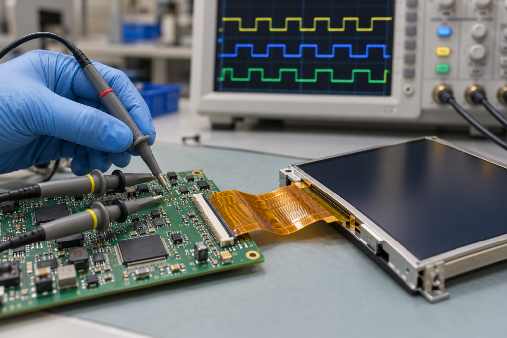
Oscilloscope probes validating signals on a TFT LCD controller board
Oscilloscope checks
On accessible parallel signals, an oscilloscope can measure Pixel Clock frequency, HSYNC rate, VSYNC rate, DE width, polarity and startup order. From the measured HSYNC and VSYNC rates, engineers can check whether the actual line and frame cadence agrees with the intended mode.
Use probes and bandwidth appropriate for the signal. Poor probing can distort an edge or add enough loading to change behavior. Differential high-speed links require suitable differential measurement equipment and methods.
Logic-analyzer checks
A logic analyzer can help with lower-speed control signals, GPIO sequencing, SPI initialization or I²C configuration. It is not automatically suitable for capturing every MIPI, LVDS or eDP physical-layer signal. Use protocol-specific equipment when the link speed and signaling method require it.
Measurement does not replace the datasheet
A measurement shows what the board generates, not what the panel accepts. Compare it with the approved specification.
Firmware, Device Tree und Board-Konfiguration
A typical embedded display configuration can include:
Aktive Breite und Höhe
Horizontale und vertikale Porches
HSYNC and VSYNC widths
Pixel Clock or clock-divider settings
HSYNC, VSYNC, DE and clock polarity
Pixel format and color order
LVDS mapping or MIPI lane settings
Reset and enable GPIO behavior
Panel-Initialisierungsbefehle
Backlight enable and dimming control
Linux display drivers and device trees often store mode parameters as separate clock, active-area, margin, sync-length and polarity values. An Android-based board can use the same kernel-level configuration concepts even though the user interface runs on Android.
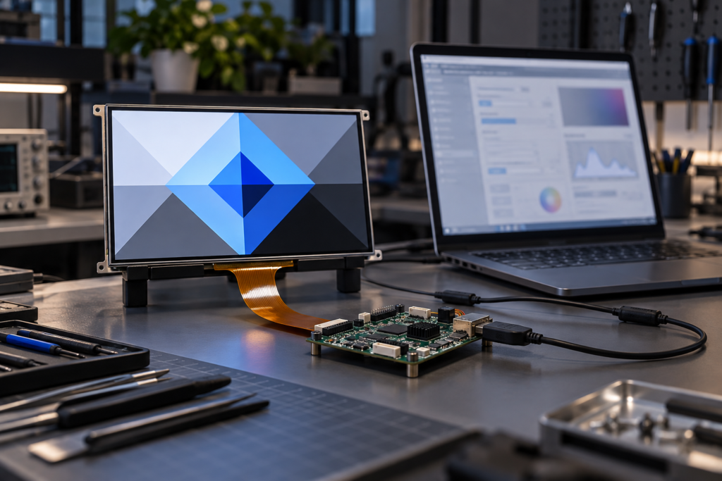
Firmware configuration test for a TFT LCD and controller board
Firmware adaptation is therefore a real part of panel matching. It should be planned with the hardware review rather than treated as a final software setting after the board is complete.
Was RJY Display prüfen kann
RJY Display can review display timing as part of a project-specific LCD and controller-board configuration. Depending on the selected panel and host platform, the scope can include:
Native resolution and timing-table comparison
Pixel Clock, porch, sync and polarity review
RGB, LVDS, MIPI, eDP and related interface coordination
Controller-board and bridge-path evaluation
Project-dependent firmware adaptation
FPC, connector and pin-definition coordination
Backlight, touchscreen and power review
Display-related mechanical integration
This is a compatibility process, not a universal board claim. The result depends on the exact LCD, controller hardware, firmware, operating system and application environment. An active HDMI-to-MIPI or HDMI-to-LVDS path must be designed for the selected panel; it is not a passive cable conversion.
Informationen, die für eine Timing-Kompatibilitätsprüfung benötigt werden
Send the following information where available:
Vollständige LCD-Modellbezeichnung und Revision
Panel datasheet and timing table
Native resolution and interface
Driver IC or timing-controller information
Pin definition and connector drawing
Pixel Clock range
Horizontal and vertical porch values
HSYNC and VSYNC widths and polarity
Controller board, processor and bridge IC
Operating system, firmware or BSP information
Backlight and touchscreen requirements
Photographs or video of the current failure
Sample quantity, expected volume and project schedule
If the current system already works with another panel, include that panel’s datasheet and approved configuration. A side-by-side comparison often shows whether the difference lies in timing, pinout, interface mode, power or software.
Vollständiges Timing verwenden, nicht nur die Auflösung
LCD pixel clock connects resolution, blanking and refresh rate, but it is not the only compatibility parameter. Engineers must also preserve the required porches, sync widths, Data Enable behavior, polarity and sampling edge. The chosen interface and firmware then need to carry or generate that mode correctly.
This is why two same-resolution panels can produce different results on the same board. Treat the panel timing table as part of the hardware specification, not as an optional software detail.
Pixel Clock is the rate at which pixel periods advance in a display timing stream. It includes active pixels and the pixel periods used by horizontal and vertical blanking.
How do I calculate LCD pixel clock?
Add the active width, horizontal porches and HSYNC width to obtain the horizontal total. Add the active height, vertical porches and VSYNC width to obtain the vertical total. Multiply both totals by the refresh rate. Then compare the result with the panel’s specified clock range.
Is pixel clock the same as refresh rate?
No. Refresh rate is the number of complete frames per second. Pixel Clock is the number of pixel periods per second. The totals for each line and frame connect the two values.
Why do two LCDs with the same resolution use different timings?
They can use different driver ICs, blanking intervals, synchronization modes, clock ranges, signal polarities and initialization requirements. Resolution describes only the active pixel matrix.
Can I change porch values if the total timing stays the same?
Do not assume so. A panel can require specific front porch, sync width and back porch ranges even when the total is unchanged. Use the exact datasheet limits and validate the complete system.
What happens when HSYNC or VSYNC polarity is wrong?
The panel may fail to recognize line or frame boundaries. Possible results include a black screen, image shift, unstable display or intermittent operation. These symptoms can also have other causes.
Does an LVDS or MIPI display still need timing configuration?
Yes. These interfaces transport display data differently from parallel RGB, but the host, bridge and panel still need a supported native mode. Link mapping, lane configuration, throughput and firmware must also match.
Can RJY match a controller board using only the LCD resolution?
No. A review also needs the LCD model, interface, pin definition, timing, driver IC when available, power, backlight, touch, firmware, operating system and application requirements.