Vous rencontrez un goulot d'étranglement dans votre projet d'affichage embarqué ?
Ne laissez pas l'intégration complexe ou les problèmes de chaîne d'approvisionnement ralentir votre mise sur le marché. Réservez une consultation gratuite avec l'équipe d'experts RJY pour un accompagnement sur mesure en conception et fabrication.
Mappage des données des écrans LCD TFT LVDS : Guide de compatibilité VESA vs JEIDA
Publié :
Lecture de 9 min
Mis à jour :
An LVDS TFT LCD can power up, lock to the incoming signal, and show a stable image while still rendering colors incorrectly. When resolution and synchronization look correct but gradients are posterized, dark tones are crushed, or colors appear unnaturally shifted, the problem may be the data mapping rather than the panel glass, cable quality, or application software.
VESA and JEIDA are commonly referenced mapping conventions for arranging RGB pixel bits across an LVDS display link. They do not change the physical connector by themselves, and they should not be confused with pixel timing, lane polarity, single- versus dual-channel LVDS, or the electrical characteristics of the interface. They define how the transmitter and receiver interpret the serialized pixel data. Both ends must agree.
This guide explains how mapping affects an embedded TFT LCD system, how to distinguish a mapping problem from other compatibility failures, and what engineers should verify before approving a replacement panel or controller-board configuration.
Figer la configuration testée
LVDS describes a low-voltage differential signaling method, but an LCD connection also needs an agreed method for transporting pixel and control information. In many flat-panel systems, a serializer converts parallel RGB data into a stream carried over differential pairs, and the panel-side receiver reconstructs the pixel data.
Texas Instruments documents multiple RGB-to-LVDS/OpenLDI mappings for 18-bit and 24-bit display paths, demonstrating that interoperability depends on assigning the correct input bits to the expected serialized outputs.1 Linux panel bindings likewise treat jeida-18, jeida-24et vesa-24 as distinct data-mapping values rather than interchangeable names.2
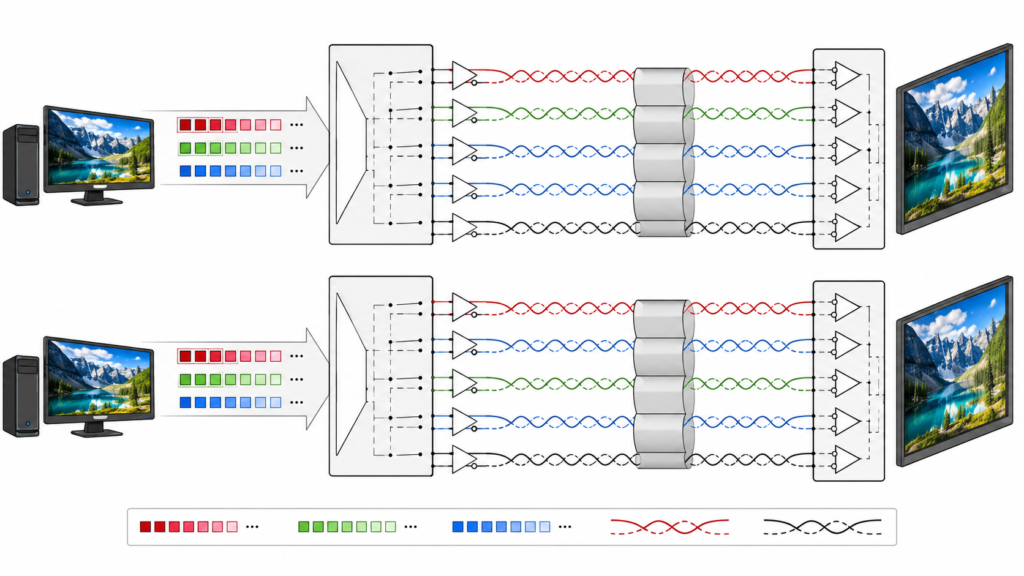
Conceptual comparison of two RGB bit-order mappings across LVDS differential lanes
This creates an important engineering distinction: a cable may have the correct connector and differential-pair count, yet the displayed colors can still be wrong because the transmitter packs pixel bits differently from the way the panel receiver expects them.
Commencer par des images de test déterminist
For an RGB888 path, each red, green, and blue component contains eight bits. Some bits carry more visual weight than others. The most significant bits determine the larger steps in intensity, while the least significant bits refine smaller differences. VESA and JEIDA mappings place these bits differently across the serialized LVDS lanes.
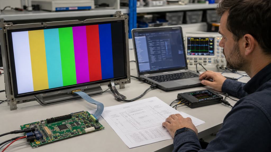
Engineer diagnosing stable but incorrect colors on an LVDS TFT LCD system
STMicroelectronics explains the practical distinction by noting that VESA groups the least significant RGB component bits on the first three data lanes, while JEIDA keeps the six most significant bits on the common three-lane portion and places the additional RGB888 bits on the fourth lane.3 This difference matters when a 24-bit transmitter and a 24-bit panel use different conventions.
Objet
What to Verify
Pourquoi c'est important
Profondeur des couleurs
RGB666 or RGB888 path
Determines the number of active color bits and commonly used data lanes
Data mapping
JEIDA or VESA convention stated by the panel and transmitter
Determines where significant and less-significant RGB bits are serialized
LVDS channel architecture
Single-channel or dual-channel implementation
Affects how pixels are divided across links; it is not the same question as VESA versus JEIDA
Lane order and polarity
Pair assignment, positive/negative polarity, connector pinout, and any mirror function
A mapping setting cannot correct arbitrary wiring or polarity errors
Pixel timing
Active area, pixel clock, sync, porches, and refresh behavior
Correct mapping does not compensate for incompatible timing
Typical Symptoms of a VESA/JEIDA Mismatch
A mapping mismatch often produces a different failure signature from missing power or incorrect timing. The panel may show a stable, correctly positioned image because the receiver is recovering the clock and control structure. However, the interpretation of color significance is wrong.
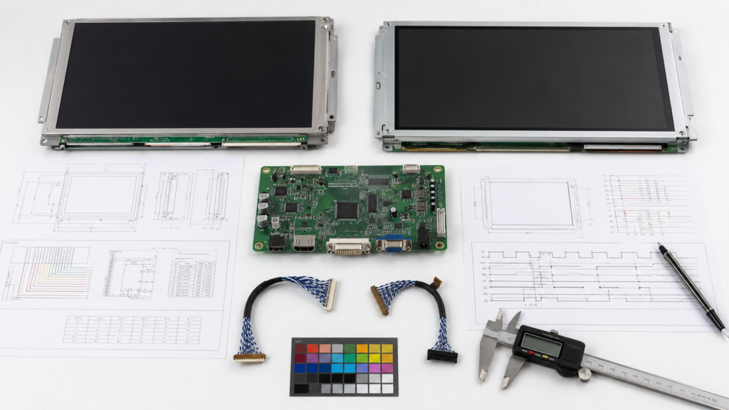
Existing and candidate LVDS TFT LCD modules under compatibility review before replacement
Common observations include:
smooth gradients becoming visibly stepped or posterized;
dark shades appearing too dark, clipped, or unexpectedly tinted;
color bars displaying the wrong intensity relationships;
photographs looking unnatural even though text and geometry remain sharp;
a replacement panel showing different color behavior while the original panel remains correct on the same host.
These symptoms are diagnostic clues, not proof. Reversed channel order, an incorrect lane assignment, a bit-depth mismatch, a bridge-register error, or a signal-integrity problem may also corrupt color. If the display has no image, unstable synchronization, an offset active area, flicker, or intermittent startup, engineers should first review power, reset, timing, cable, signal integrity, and initialization rather than assuming a VESA/JEIDA issue.
How to Verify Mapping Before Connecting a New Panel
The safest source is the complete panel specification, not a distributor summary or connector photograph. Locate the LVDS input section and identify the actual mapping diagram. The word “LVDS” alone is insufficient.
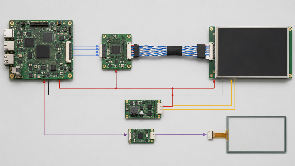
Embedded LVDS display architecture with separate video, backlight, power and touch paths
Check the Panel Documentation
Confirm the color depth, data-pair count, clock pair, single- or dual-channel architecture, connector pinout, polarity, timing table, power rails, enable sequence, backlight requirements, and the bit mapping expected by the panel. Some documents state VESA or JEIDA directly. Others provide only a slot-by-slot diagram that must be compared with the transmitter documentation.
Do not rely only on bit labels such as R0 or R7 without reading the manufacturer’s convention. ST notes that some panel specifications label the most significant and least significant bits in ways that can create confusion.4 The diagram and explanatory notes should control the interpretation.
Check the Transmitter, Bridge, or SoC Output
The host may contain a native LVDS transmitter, an RGB-to-LVDS serializer, a MIPI DSI-to-LVDS bridge, or another active conversion device. Verify whether its mapping is fixed, selected by a pin, changed through registers, or configured in firmware. Linux device-tree bindings expose mapping as an explicit property for relevant LVDS panels and codecs, which reinforces that the setting belongs in the controlled hardware/software configuration.5 For the wider system-level review, see RJY Display’s guide to matching a TFT LCD module with an Android control board.
If the source is HDMI, an active receiver or scaler must first convert the video into a panel-compatible path. A passive HDMI-to-LVDS cable cannot create the required receiver, timing, mapping, panel power, or backlight functions.
A Practical LVDS Mapping Diagnosis Workflow
1. Freeze the Tested Configuration
Record the panel model and revision, controller-board revision, bridge or serializer part, firmware or BSP build, cable drawing, jumper states, and relevant register or device-tree settings. Without configuration control, a corrected prototype can later fail again after a board or software revision.
2. Start With Deterministic Test Images
Use full-intensity red, green, blue, white, and black fields together with grayscale ramps and channel gradients. A photograph may reveal that the image looks wrong, but controlled patterns make it easier to distinguish component order, bit significance, clipping, and missing shades.
3. Confirm Timing and Electrical Stability
Verify that the active resolution, pixel clock, synchronization, power sequence, reset, enable, and backlight behavior comply with the panel specification. Confirm the differential-pair routing and connector pinout. Do not use a mapping change to hide a wiring or timing fault.
4. Compare the Two Mapping States Deliberately
Si l'émetteur prend en charge les deux mappages, modifiez uniquement la commande de mappage tout en maintenant constants le motif de test, la synchronisation, le câble et la configuration d'alimentation. Une comparaison A/B contrôlée est plus fiable que la modification simultanée de plusieurs registres du pont.
5. Validate More Than the Boot Screen
Testez l'interface utilisateur normale de l'application, les dégradés, les images, la suspension/reprise, le démarrage à froid, le redémarrage à chaud, les transitions de luminosité et tous les modes de fonctionnement requis. Un logo de démarrage correct ne prouve pas que chaque état d'affichage et chemin logiciel utilise la même configuration.
6. Lock the Mapping Into Production Documentation
Ajoutez le mappage approuvé à la matrice de compatibilité panneau-carte de contrôle, au schéma de câblage, au manifeste du firmware, à la source de l'arborescence des périphériques, à la procédure de test de production et au registre de contrôle des modifications. Traitez un changement de mappage comme un changement de compatibilité, et non comme une préférence logicielle cosmétique.
Why Mapping Matters During LVDS Panel Replacement
Les projets de remplacement de panneaux commencent souvent par la taille mécanique, la résolution, le type de connecteur, la luminosité et la disponibilité. Ces vérifications sont nécessaires mais insuffisantes. Deux panneaux aux dimensions similaires et avec la même interface LVDS nominale peuvent présenter une profondeur de couleur, un mappage, une architecture de canaux, une synchronisation, un brochage, une alimentation ou un contrôle du rétroéclairage différents. Le guide de RJY Display pour remplacer un module d'affichage TFT LCD discontinué explique le processus plus large de forme, d'ajustement, de fonction, de cycle de vie et de qualification.
Vérification du remplacement
Ne présumez pas
Preuves requises
Connecteur
Un même connecteur signifie un même brochage
Les deux tableaux de connecteurs et le schéma de câblage
Mappage LVDS
Tous les panneaux LVDS 24 bits utilisent un seul format
Schéma de mappage du panneau et configuration de l'émetteur
Calendrier
Une même résolution signifie une synchronisation identique
Horloge pixel, porche, synchronisation et plages de rafraîchissement
Alimentation et rétroéclairage
L'hôte peut réutiliser chaque rail et signal d'activation
Séquence d'alimentation, exigences de tension/courant et spécification du rétroéclairage
Logiciels
Le firmware existant identifiera et pilotera automatiquement le panneau
Révision du pont, du pilote, de l'arborescence des périphériques et de l'image de production
Pour un programme de remplacement OEM, l'objectif approprié n'est pas de trouver un panneau qui semble similaire. Il s'agit de qualifier une configuration contrôlée complète : panneau, câble, contrôleur ou pont, firmware, alimentation, rétroéclairage, assemblage mécanique et preuves de validation.
Information to Provide for an LVDS Compatibility Review
Pour examiner efficacement un projet d'affichage LVDS, fournissez le modèle et la fiche technique du panneau actuel, la documentation du panneau candidat, les informations sur l'hôte ou la carte de contrôle, le schéma de câblage, la résolution et le comportement de rafraîchissement requis, les détails du pont ou du sérialiseur, la version du système d'exploitation ou du firmware, les exigences de rétroéclairage, le dessin mécanique, le volume annuel, la quantité de prototypes et des photographies du défaut d'image actuel si un dépannage est nécessaire.
RJY Display peut évaluer les modules d'affichage TFT LCD disponibles et les options de carte de contrôle par rapport à une exigence de projet définie. L'examen doit commencer par une plateforme de panneau existante et des besoins de compatibilité documentés, plutôt que par l'hypothèse qu'un panneau LVDS peut être rendu interchangeable par un simple changement de câble. Pour une frontière de personnalisation plus large, consultez le guide d'ingénierie des TFT LCD personnalisés.
Les connecteurs physiques VESA et JEIDA sont-ils différents ?
Non. Les mappages VESA et JEIDA décrivent comment les données de pixels sont organisées sur un chemin d'affichage LVDS. Le type de connecteur et le brochage sont des exigences de compatibilité distinctes.
L'image peut-elle rester stable lorsque le mappage LVDS est incorrect ?
Oui. Le panneau peut récupérer l'horloge et afficher une géométrie stable tandis que les couleurs, les dégradés et les niveaux d'intensité sont incorrects car les bits RVB sont interprétés aux mauvaises positions.
Un logiciel peut-il corriger une incompatibilité entre VESA et JEIDA ?
Uniquement si l'émetteur LVDS, le pont ou le contrôleur d'affichage prend en charge le changement de mappage via un réglage matériel ou logiciel documenté. La correction des couleurs au niveau de l'application n'est pas un substitut fiable à la configuration du mappage réel du sérialiseur.
VESA par rapport à JEIDA est-il la même chose que LVDS monocanal par rapport à double canal ?
Non. Le mappage définit l'organisation des bits de pixels. Les architectures monocanal et double canal décrivent comment les données d'affichage sont réparties sur une ou deux liaisons LVDS. Les deux doivent être vérifiés indépendamment.
Que faut-il tester après avoir changé un panneau LVDS ?
Validez le mappage, les rampes de couleurs, les champs de couleurs pleines, la synchronisation, le démarrage, le redémarrage, la suspension/reprise, la séquence d'alimentation, le contrôle du rétroéclairage, l'intégrité du câble, l'interface utilisateur complète de l'application, l'assemblage mécanique et chaque mode de fonctionnement requis.
Partagez la taille de votre écran, sa résolution, son interface, sa luminosité, ses exigences tactiles, les besoins en carte contrôleur et l'environnement d'application.