Facing a bottleneck in your Embedded Display Project?
Don’t let complex integration or supply chain issues slow your time-to-market. Book a free consultation with the RJY expert team for tailored design and manufacturing support.

Thin-Film Transistor Liquid Crystal Displays (TFT-LCDs) have become the cornerstone of modern display technology, powering everything from smartphones and televisions to computer monitors and automotive displays. However, the manufacturing process behind these displays is highly intricate, involving several critical steps that ensure high-quality performance. In this article, we will delve into the key stages of TFT-LCD manufacturing, from array creation to cell fabrication and final module assembly.
TFT-LCD manufacturing is a multi-stage process that turns glass, thin-film transistors, liquid crystal material, color filters, polarizers, driver circuits, backlight components, and mechanical parts into a working display module. For engineers and B2B buyers, understanding this process helps explain why display selection is not only about size and resolution. It also affects interface compatibility, brightness, touch integration, mechanical structure, reliability, lead time, and customization feasibility.
A TFT-LCD is not manufactured as one simple part. It is typically built through three major stages: array manufacturing, cell assembly, and module assembly. The array process creates the thin-film transistor backplane. The cell process combines the TFT array glass, color filter glass, and liquid crystal layer. The module process integrates polarizers, driver ICs, FPC, backlight, frame, and other components into a usable LCD module.
This guide explains the main manufacturing processes for TFT-LCDs and how each stage affects the final display module used in embedded devices, industrial HMIs, smart home panels, vehicle-related displays, security equipment, and other B2B products.
TFT-LCD stands for thin-film transistor liquid crystal display. It is a type of active-matrix LCD. A TFT-LCD uses a thin-film transistor structure to control individual pixels or subpixels more precisely than older passive-matrix LCD designs.
The liquid crystal layer does not emit light by itself. Instead, it controls how light passes through the display structure. In most modern TFT-LCD modules, an LED backlight provides the light source. The TFT array controls pixel behavior, the liquid crystal layer modulates light, and the color filter creates red, green, and blue subpixels.
A finished TFT-LCD module may include the LCD cell, polarizers, driver IC, FPC, backlight unit, metal or plastic frame, touch panel, cover glass, and sometimes a controller board depending on the product design.
The TFT-LCD manufacturing process is commonly divided into three main stages:
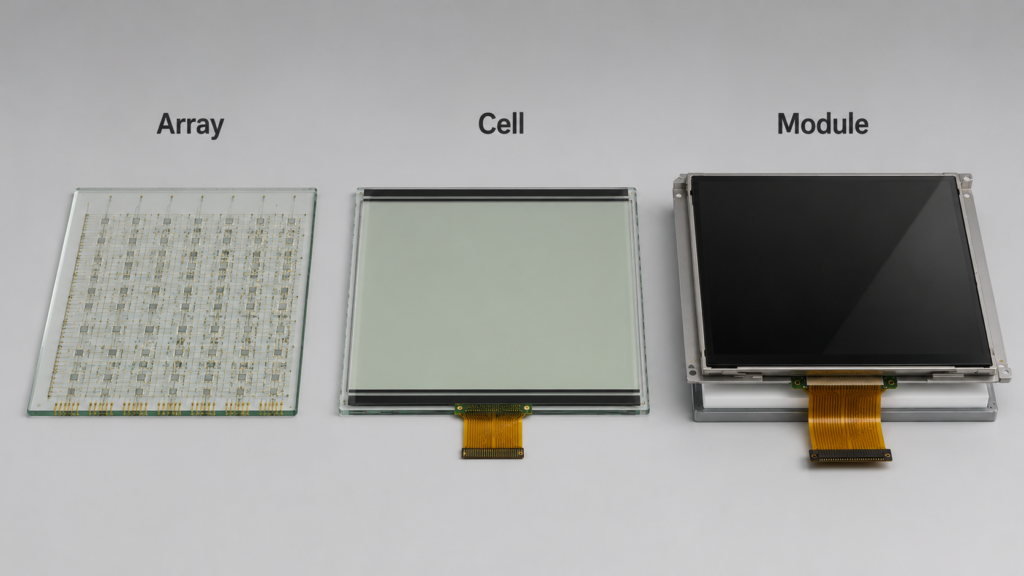
These three stages define the basic structure of the final display. The array process affects pixel control and electrical performance. The cell process affects optical performance and image formation. The module process affects brightness, interface, mechanical fit, touch integration, and final usability.
| Manufacturing Stage | Main Purpose | Key Output |
|---|---|---|
| Array process | Build the TFT transistor matrix on glass | TFT array substrate |
| Cell process | Join TFT glass, color filter glass, and liquid crystal layer | LCD cell |
| Module process | Add polarizers, ICs, FPC, backlight, frame, and related parts | Finished TFT-LCD module |
The array process is the foundation of TFT-LCD manufacturing. In this stage, a thin-film transistor matrix is formed on a glass substrate. This matrix controls how pixels respond to electrical signals.
The process is similar in concept to semiconductor manufacturing, but it is performed on large glass substrates rather than silicon wafers. The glass is cleaned, coated, patterned, etched, and processed repeatedly to create the required thin-film transistor structure, electrodes, signal lines, and storage capacitors.
Typical array manufacturing steps include:
These steps may be repeated several times because the TFT array contains multiple patterned layers. Each layer must align accurately with the previous layers. Small defects in this stage can affect pixels, lines, uniformity, yield, and display reliability.
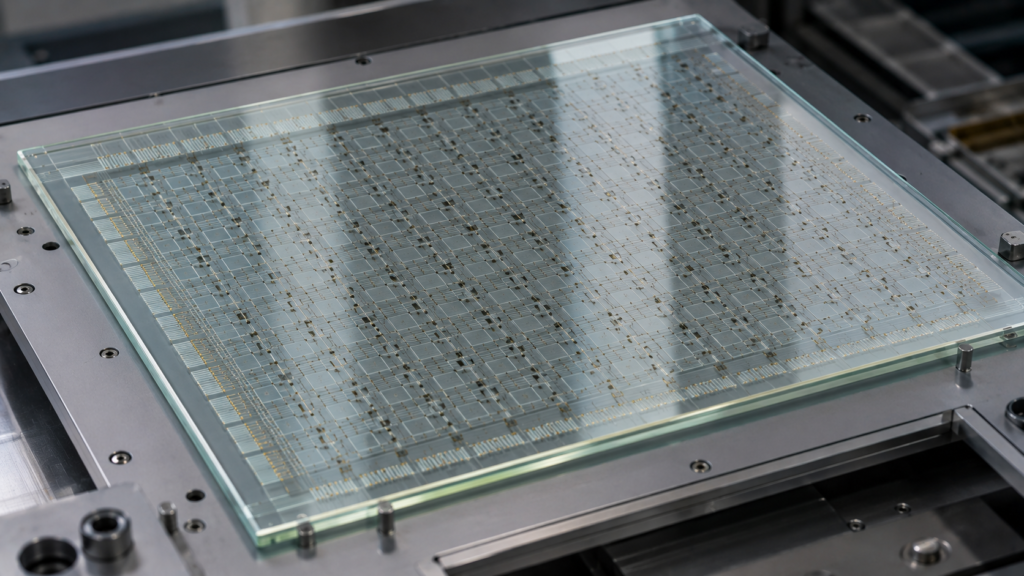
The array process determines the electrical control structure of the display. If the TFT array has defects, the finished display may show dead pixels, line defects, unstable brightness, poor image response, or other visible problems.
For buyers, this stage explains why pixel quality and panel yield are important. Even though the end user does not see the TFT array directly, it is responsible for precise pixel control. A high-quality TFT backplane supports stable image display, higher resolution, and more consistent performance.
In practical product selection, the buyer does not usually control the array process directly. However, understanding it helps explain why display modules from different sources may vary in consistency, yield, and long-term performance even if the basic size and resolution look similar.
A color TFT-LCD also needs a color filter substrate. The color filter glass contains red, green, and blue filter patterns that allow the display to create full-color images.
The color filter process forms tiny red, green, and blue areas aligned with the pixel structure. It also includes black matrix areas that help separate subpixels and improve contrast. The color filter substrate must later be aligned with the TFT array substrate during cell assembly.
Color filter quality affects color appearance, brightness, contrast, and uniformity. If the color filter pattern is poorly aligned or inconsistent, the final image may show color shift, reduced sharpness, or optical defects.
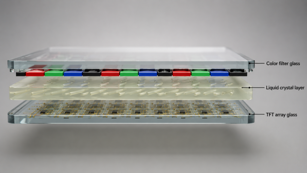
The cell process combines the TFT array substrate and the color filter substrate. Liquid crystal material is placed between these two glass substrates, creating the optical core of the LCD.
Important cell assembly steps include:
The gap between the two glass substrates must be controlled carefully. This cell gap affects optical performance, response behavior, color uniformity, and viewing quality. The liquid crystal material must also be distributed consistently across the active display area.
The cell process is where the display begins to behave like an LCD. Before this stage, the TFT array and color filter are separate glass substrates. After cell assembly, the structure can modulate light through the liquid crystal layer.
Cell assembly quality can affect viewing angle, contrast, response time, mura, light leakage, and uniformity. Many visible display defects are related to glass alignment, liquid crystal distribution, cell gap control, contamination, or mechanical stress.
For embedded and industrial display projects, this stage also explains why the LCD cell must be protected properly during later integration. Pressure, bending, impact, or uneven mechanical stress can affect the display area and create visible marks or defects.
Polarizers are attached to the outside surfaces of the LCD cell. They are essential because liquid crystal displays work by controlling the polarization of light.
Without polarizers, the liquid crystal layer cannot form a usable visible image in the normal LCD structure. The polarizers must be applied cleanly and accurately. Dust, bubbles, scratches, or alignment errors can affect appearance and yield.
Polarizer selection also affects viewing angle, brightness, contrast, and surface appearance. In some projects, additional optical films, anti-glare layers, or surface treatments may be used depending on the application.
The LCD cell needs driver ICs to send electrical signals to the display pixels. Driver IC bonding connects the display glass to the electronics that control rows, columns, and image signals.
Common bonding methods include chip-on-glass, chip-on-film, or related assembly structures depending on the module design. The bonding area must be reliable because poor bonding can cause missing lines, partial image loss, unstable display behavior, or complete failure.
For B2B projects, this stage is closely related to interface and FPC design. The display module must match the host system or controller board in resolution, signal format, timing, voltage, pin definition, and backlight requirements.
Many TFT-LCD modules use an FPC, or flexible printed circuit, to connect the display to a mainboard or controller board. The FPC may carry display signals, power, backlight connections, touch signals, and control lines depending on the module design.
FPC design affects integration. Important details include connector type, pin pitch, bending direction, cable length, pin definition, mechanical clearance, and assembly tolerance.
For custom display projects, FPC customization may be considered when the standard module does not fit the product structure. However, FPC changes must be reviewed carefully because they can affect signal quality, mechanical reliability, and production cost.
Since a transmissive TFT-LCD does not emit light by itself, it normally requires a backlight unit. In modern modules, the backlight is usually based on LEDs.
A typical backlight unit may include LEDs, light guide plate, diffuser sheets, prism films, reflector, frame, and related electrical connections. The purpose is to distribute light evenly across the display area.
Backlight design affects:
For high-brightness or industrial applications, backlight design becomes especially important. Higher brightness may require more power and better thermal design. It should not be treated as a simple brightness number only.
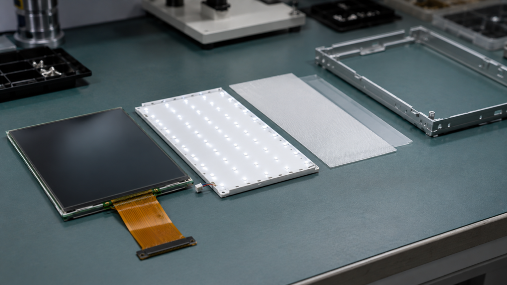
Module assembly turns the LCD cell into a usable TFT-LCD module. At this stage, the LCD cell, polarizers, driver ICs, FPC, backlight unit, frame, adhesive parts, and other mechanical components are assembled together.
Depending on the product, module assembly may also include touch panel attachment, cover glass integration, protective film, mounting structure, or interface adapter parts.
A finished module must be mechanically stable and electrically functional. The assembly must protect the LCD cell while allowing the display to fit into the target product or equipment.
Many modern TFT-LCD modules are used with touch panels. The touch layer may be resistive or capacitive depending on the application. A cover glass may also be added for protection, appearance, and front-panel integration.
Touch and cover glass integration must consider:
The touch panel is not only a surface accessory. It affects user experience, mechanical design, interface requirements, firmware or driver support, and final product reliability.
Testing and inspection are required throughout the TFT-LCD manufacturing process. Some tests happen during array and cell production. Others happen after module assembly.
Common inspection items may include:
Testing helps detect defects before the module is shipped or integrated into the customer’s product. For B2B projects, testing requirements should match the application. A consumer display, an industrial HMI, a medical-related interface, and a vehicle-related device may not have the same evaluation priorities.
Not every TFT-LCD feature is equally easy to customize. Some features are tied to the original LCD panel manufacturing process, while others can be adjusted at the module or integration level.
For many B2B projects, customization is most practical when it starts from an existing display module and adjusts related parts around it. This may include cover glass, backlight, touch panel, FPC, interface, controller board, firmware, or mechanical structure coordination.
| Customization Area | Typical Manufacturing Stage | Practical Notes |
|---|---|---|
| Resolution | Panel design and array process | Usually tied to existing panel platform |
| Display size | Panel design and cutting plan | New sizes from scratch are complex and not always practical |
| Brightness | Backlight and module design | Often more practical than changing the LCD cell itself |
| FPC shape or pinout | Module assembly and electrical design | Requires compatibility and reliability review |
| Touch panel | Module integration | Can be reviewed based on touch type and use environment |
| Cover glass | Module integration | Common for front-panel and product appearance requirements |
| Controller board | System integration | Depends on panel interface, resolution, timing, firmware, and application |
| Firmware | Controller board and system level | Project-dependent and requires technical communication |
Most buyers do not need to manage the full TFT-LCD production process. However, understanding the process helps buyers ask better questions and avoid unrealistic expectations.
For example, changing cover glass is very different from developing a new LCD panel size. Adjusting backlight brightness is different from changing resolution. Matching a controller board is different from changing the TFT array. Each request belongs to a different technical layer and may have different cost, timing, and feasibility implications.
Understanding the manufacturing process helps buyers evaluate:
One common mistake is assuming that all display features can be changed easily. In reality, resolution, active area, glass size, and pixel structure are usually tied to the original panel platform.
Another mistake is treating the backlight as a minor accessory. Backlight design affects brightness, heat, power consumption, thickness, and visibility. For industrial and high-brightness applications, it is a major design factor.
A third mistake is ignoring FPC and connector details. Even if the display size and resolution match, an incompatible FPC, pin definition, voltage requirement, or interface can prevent the module from working with the customer’s system.
A fourth mistake is waiting until late development to consider touch panel and cover glass design. Touch and cover glass affect mechanical structure, user experience, optical performance, and assembly planning.
To evaluate a TFT-LCD project efficiently, buyers should prepare enough technical information before inquiry. The more complete the information, the faster a supplier can confirm feasibility.
Useful project information includes:
This information helps clarify whether the project can use an existing module, needs module-level customization, or requires deeper engineering review.
RJY Display supports TFT LCD modules, controller boards, and custom display solution discussions for engineering-driven B2B projects. The practical engineering path is usually to start from an existing display module and review the related customization areas around it.
Project support may involve display size selection, resolution review, interface matching, brightness customization, backlight review, touch panel integration, cover glass design, FPC discussion, controller board matching, firmware support, and mechanical structure coordination.
If your project needs a TFT-LCD module, touch display, high-brightness display, controller board, or custom display support, prepare your display requirements before inquiry so the technical review can start from accurate project information.
Send Your TFT-LCD Project Requirements
The manufacturing processes for TFT-LCDs can be understood through three major stages: array manufacturing, cell assembly, and module assembly. The array process creates the TFT backplane. The cell process combines the TFT glass, color filter glass, and liquid crystal layer. The module process integrates polarizers, driver ICs, FPC, backlight, frame, touch panel, cover glass, and other functional parts.
For B2B buyers, this process explains why display selection requires more than choosing a size and resolution. Some features are defined by the panel platform, while others can be adjusted through module design, backlight design, touch integration, controller board matching, or firmware support.
The right TFT-LCD project starts with clear requirements: size, resolution, interface, brightness, touch, cover glass, FPC, backlight, controller board, firmware, operating environment, and production expectations. Understanding the manufacturing process helps buyers communicate these requirements more clearly and make better display decisions.
The main TFT-LCD manufacturing processes are array manufacturing, cell assembly, and module assembly. Array manufacturing creates the TFT backplane, cell assembly forms the LCD cell, and module assembly integrates the backlight, polarizers, driver ICs, FPC, frame, and related parts.
The TFT array process creates the thin-film transistor matrix on a glass substrate. It involves repeated steps such as cleaning, deposition, photoresist coating, exposure, development, etching, and inspection.
LCD cell assembly combines the TFT array glass, color filter glass, and liquid crystal material. This stage forms the optical core of the LCD panel.
Module assembly integrates the LCD cell with polarizers, driver ICs, FPC, backlight unit, frame, and sometimes touch panel or cover glass. This turns the LCD cell into a usable display module.
Resolution is usually tied to the LCD panel platform and TFT array design. For many projects, it is more practical to select an existing resolution and customize related module parts such as backlight, touch panel, cover glass, FPC, controller board, or firmware.
The backlight affects brightness, uniformity, power consumption, heat, thickness, and readability. It is especially important for high-brightness, industrial, outdoor, or semi-outdoor display applications.
Useful information includes display size, resolution, interface, brightness, touch requirement, cover glass requirement, FPC requirement, backlight requirement, controller board requirement, operating environment, mechanical structure, sample needs, and expected production volume.
Share your display size, resolution, interface, brightness, touch requirement, controller board requirement, and application environment.
Continue reading related display technology guides and application references.


Explore product pages related to this article topic.

Talk to RJY’s engineering team for display matching, controller board review, and customization discussion.