¿Enfrenta un cuello de botella en su proyecto de pantalla integrada?
No permita que la integración compleja o los problemas de la cadena de suministro retrasen su tiempo de comercialización. Reserve una consulta gratuita con el equipo experto de RJY para obtener soporte personalizado en diseño y fabricación.
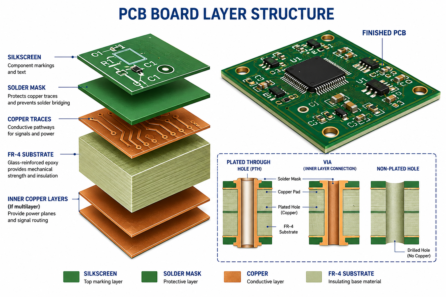
A PCB board, or printed circuit board, is made from several material layers that work together to support and connect electronic components. A typical PCB includes an insulating base material, copper conductive layers, solder mask, silkscreen marking, plated holes, and a surface finish. In an assembled PCB, components such as ICs, connectors, resistors, capacitors, LEDs, and power devices are mounted onto the board.
For display products, PCB material selection matters because the board may control LCD signals, power the backlight, connect touch panels, manage interfaces, or serve as part of a controller board. A PCB used in a simple low-speed circuit does not have the same requirements as a PCB used for MIPI, LVDS, HDMI, USB, backlight driving, or Android controller board applications.
This article explains what a PCB board is made of, how each material works, and what B2B buyers should understand when evaluating LCD controller boards, display modules, and pantalla personalizada electronics.
What Is a PCB Board?
A PCB board is a physical platform that mechanically supports electronic components and electrically connects them through copper traces. Instead of using loose wires between every component, the circuit pattern is built into the board itself.
The term PCB is often used loosely. Strictly speaking, a bare PCB is the board before components are mounted. Once electronic components are soldered onto it, it is often called a PCB assembly, PCBA, or assembled circuit board.
In display systems, a PCB may appear in several places. It may be part of an LCD controller board, a backlight driver board, a touch control board, a power board, an adapter board, or an integrated mainboard. The PCB material and layout affect signal quality, reliability, heat dissipation, connector durability, and manufacturing consistency.
Main Materials in a PCB Board
A standard rigid PCB usually contains these main material categories:
Base substrate or laminate
Copper foil or copper layers
Prepreg bonding material in multilayer boards
Solder mask
Silkscreen marking ink
Surface finish on exposed copper pads
Plated through holes and vias
Mounted electronic components in a PCB assembly
Each material has a different function. The base substrate provides insulation and mechanical strength. Copper carries electrical signals and power. Solder mask protects the copper pattern. Silkscreen helps identify components and test points. Surface finish protects exposed copper and supports solderability.
FR-4: The Most Common PCB Base Material
FR-4 is the most common base material used in many rigid PCBs. It is a glass-reinforced epoxy laminate. In simple terms, it combines woven fiberglass cloth with epoxy resin to create a strong insulating board material.
The base material must support the copper circuit, resist mechanical stress, provide electrical insulation, and tolerate manufacturing heat. FR-4 is widely used because it offers a practical balance of cost, mechanical strength, insulation performance, and manufacturability. However, FR-4 is not one single performance level. Different FR-4 materials may have different glass transition temperatures, dielectric properties, thermal performance, and suitability for lead-free soldering or higher-frequency signals.
For ordinary low-to-medium-speed electronic boards, standard FR-4 may be enough. For high-speed display interfaces, power-heavy designs, or demanding industrial environments, the specific laminate grade should be reviewed more carefully.
Copper Layers: The Conductive Part of the PCB
Copper is the main conductive material in a PCB. It forms the traces, pads, planes, and vias that connect electronic components. Copper may appear on one side, both sides, or multiple internal layers of the board.
A simple single-sided PCB has copper on one side. A double-sided PCB has copper on both sides. A multilayer PCB has copper layers inside the board as well as on the outer surfaces. Multilayer construction is common when a circuit needs higher density, better grounding, controlled impedance, or separation between power and signal layers.
PCB board material layer structure showing FR-4 substrate copper traces solder mask silkscreen vias and plated holes
In display controller boards, copper layers may carry high-speed signals, power rails, ground planes, backlight current, touch interface signals, and connector routing. The thickness, width, spacing, and layer stack-up of the copper traces influence performance and reliability.
Prepreg and Core Materials in Multilayer PCBs
In multilayer PCBs, the board is not just one flat sheet. It is built from cores and prepreg layers. A core is a cured laminate layer with copper. Prepreg is a resin-impregnated fiberglass material that bonds layers together during lamination.
During manufacturing, heat and pressure bond the layers into one solid structure. The final stack-up may include signal layers, ground planes, power planes, and controlled-impedance layers.
Infographic showing FR-4 substrate copper layer solder mask and surface finish materials in a PCB board
This is important for high-speed display and controller board applications. Interfaces such as LVDS, HDMI, USB, eDP, and MIPI-related circuits may require careful stack-up design, impedance control, ground reference, and differential pair routing. The PCB material is therefore part of signal performance, not only a mechanical carrier.
Solder Mask: The Protective Coating
Solder mask is the colored protective coating commonly seen on PCB surfaces. Green is the most common color, but solder mask can also be black, blue, red, white, or other colors depending on the project.
The solder mask covers most copper areas while leaving pads exposed where components need to be soldered. It helps prevent solder bridges, protects copper from oxidation, improves insulation between traces, and makes the board more durable during handling and assembly.
In display control boards, solder mask quality matters around fine-pitch connectors, IC pins, FPC connectors, touch connectors, and high-density component areas. Poor solder mask registration or weak adhesion can create manufacturing and reliability problems.
Silkscreen: The Printed Marking Layer
Silkscreen is the printed marking layer on the PCB. It may include component reference designators, polarity marks, connector labels, test point labels, warning marks, production codes, or assembly guidance.
Silkscreen does not carry electrical signals. Its value is practical. It helps engineers, assembly workers, repair technicians, and quality inspectors identify the board layout more quickly.
For controller boards, clear connector labeling can reduce installation errors. This is useful when a board includes LCD connector, touch connector, power input, backlight output, USB, HDMI, LVDS, MIPI, UART, speaker, or other interfaces.
Surface Finish: Protecting Exposed Copper Pads
Exposed copper oxidizes easily. A PCB surface finish protects exposed pads and supports soldering. Common surface finishes include HASL, lead-free HASL, ENIG, OSP, immersion silver, and immersion tin.
The choice affects solderability, shelf life, flatness, cost, and suitability for fine-pitch components. For dense controller boards with fine-pitch ICs, connectors, or high-reliability assembly needs, surface finish selection can matter.
Buyers do not always need to specify the surface finish themselves. However, if a project involves fine-pitch connectors, long storage, repeated production, or strict assembly requirements, the supplier should select and control the finish appropriately.
Vias and Plated Holes
Vias are plated holes that connect copper layers inside a PCB. They allow signals or power to move from one layer to another. Through-hole vias pass through the entire board, while blind and buried vias are used in more complex multilayer boards.
Plated through holes are also used for through-hole components, connectors, and mechanical mounting points. In many display controller boards, connectors and power terminals may require strong mechanical support and reliable plating.
Via design affects signal routing, power delivery, heat transfer, and manufacturing cost. For high-speed or compact boards, via placement can also affect signal integrity.
Electronic Components on a PCB Assembly
A PCB board becomes a functional electronic module only after components are assembled onto it. These components may include:
Microprocessors or controller ICs
Memory chips
Power management ICs
Backlight driver ICs
Voltage regulators
Resistors and capacitors
Crystal oscillators
Connectors and FPC sockets
USB, HDMI, LVDS, MIPI, eDP, or other interface components
Touch controller circuits
Protection components such as ESD diodes
For LCD display projects, the assembled board may handle image input, display timing, touch data, power conversion, firmware behavior, backlight control, and communication with the host system.
What Is a PCB Stack-Up?
A PCB stack-up is the arrangement of copper layers, insulating layers, prepreg, and cores inside the board. Stack-up design determines how signals, power, and ground are arranged.
A simple two-layer PCB may have copper on the top and bottom with FR-4 between them. A four-layer PCB may include top signal layer, inner ground layer, inner power layer, and bottom signal layer. More complex boards may use six, eight, or more layers.
Stack-up matters for display controller boards because interfaces such as USB, HDMI, LVDS, eDP, and MIPI-related signal paths may require controlled impedance and stable reference planes. A poor stack-up can cause signal integrity problems even when the schematic is correct.
Common PCB Material Structure
PCB Part
Common Material
Main Function
Base substrate
FR-4 glass-reinforced epoxy laminate
Provides insulation and mechanical support
Copper layer
Copper foil or plated copper
Conducts signals, power, and ground
Prepreg
Resin-impregnated fiberglass
Bonds layers in multilayer boards
Solder mask
Polymer coating
Protects copper and prevents solder bridging
Silkscreen
Printed marking ink
Shows labels, part references, polarity, and assembly marks
Surface finish
ENIG, HASL, OSP, immersion tin, or other finish
Protects exposed copper and supports soldering
Vias and plated holes
Plated copper inside holes
Connects layers and supports through-hole mounting
Rigid PCB, Flexible PCB, and Rigid-Flex PCB
Not all PCBs are rigid boards. Different electronic products may use rigid PCBs, flexible PCBs, or rigid-flex PCBs.
A rigid PCB uses a stiff base material such as FR-4. This is common for controller boards, power boards, and mainboards.
A flexible PCB, often called FPC, uses a flexible base material such as polyimide. FPCs are common in LCD modules, touch panels, camera modules, and compact electronics where the circuit must bend or fit into limited space.
A rigid-flex PCB combines rigid sections and flexible sections in one integrated structure. It can reduce connectors and improve compactness, but it is usually more expensive and requires more careful design.
In LCD products, the display module may include a flexible printed circuit connected to the glass cell, while the controller board may be a rigid PCB. The connection between the display FPC and the controller board is a common integration point that must be checked carefully.
PCB Materials in LCD Controller Boards
An LCD controller board is not just a generic PCB. It may need to support display input, timing conversion, backlight driving, touch communication, power regulation, firmware control, and external interfaces.
For example, a controller board may include HDMI input, USB touch, LVDS output, MIPI interface, eDP interface, audio, backlight output, or power input. These functions place different requirements on the PCB material, layer count, routing, grounding, connector placement, and component selection.
If the board carries high-speed differential signals, the PCB material and stack-up should support controlled impedance. If it handles backlight power, copper width and thermal design matter. If it connects to an FPC, connector selection and mechanical stability matter.
How PCB Material Affects Display Performance
PCB material and layout can affect display performance indirectly. A poor PCB design may cause unstable power, signal noise, weak grounding, connector issues, backlight flicker, touch interference, or display initialization failure.
Multilayer PCB stack-up illustration showing signal layers ground plane power plane vias and controlled impedance display routing
For high-speed display interfaces, signal integrity is especially important. The board must route signals with appropriate impedance, spacing, length control, reference planes, and grounding. The selected laminate, copper thickness, layer stack-up, and connector structure all contribute to the final result.
For industrial or long-term equipment projects, the PCB should also support stable manufacturing and repeat production. Material changes, stack-up changes, connector substitutions, or uncontrolled component alternatives can affect consistency.
PCB Material and Heat Management
PCBs also play a role in heat management. Copper conducts heat as well as electricity. Wider copper areas, copper planes, thermal vias, and board layout can help distribute heat away from power components.
Display controller boards may include power regulators, backlight driver circuits, processors, memory, and interface chips. These components can generate heat. If the thermal design is weak, the board may become unstable or affect long-term reliability.
For high-brightness displays, backlight driving is an important thermal consideration. The PCB and controller board design should be reviewed together with brightness requirement, backlight current, enclosure structure, and operating environment.
PCB Materials and Compliance
PCB materials and assemblies may need to meet regional material restrictions. RoHS is one of the most common requirements for electrical and electronic equipment in many markets. It restricts certain hazardous substances such as lead, mercury, cadmium, hexavalent chromium, PBB, PBDE, and several phthalates.
Compliance should not be assumed based only on appearance. Buyers should confirm whether the specific board, components, soldering process, surface finish, cable, connector, and display module meet the applicable requirements for the final product and target market.
For B2B projects, documentation matters. If the final product is sold into Europe, North America, Japan, South Korea, or other regulated markets, the buyer should clarify what material declarations or compliance documents are required before mass production.
Common PCB Board Types by Layer Count
PCB Type
Estructura
Uso típico
Single-sided PCB
Copper on one side
Simple low-cost circuits
Double-sided PCB
Copper on both sides
Moderate complexity circuits
Four-layer PCB
Outer signal layers plus internal power or ground layers
Controller boards, compact electronics, better signal routing
Six-layer or higher PCB
Multiple signal, power, and ground layers
High-density, high-speed, or processor-based boards
Flexible PCB
Flexible base material and copper traces
LCD FPC, touch panels, compact connections
Rigid-flex PCB
Rigid and flexible areas combined
Compact devices with complex mechanical constraints
What Should Buyers Check in a PCB or Controller Board?
When evaluating a PCB board or LCD controller board, buyers should look beyond the board material name. The PCB must match the electrical, mechanical, thermal, and compliance requirements of the complete product.
Useful questions include:
What is the PCB layer count?
What base material is used?
Does the design require controlled impedance?
What display interface does the board support?
Does the board support the required LCD resolution and timing?
What connectors are used for the LCD, touch panel, and power input?
What are the backlight voltage and current requirements?
Does the board require firmware customization?
Is the board suitable for the target operating environment?
Are material compliance documents required?
Is the board sold separately or as part of a display solution?
Common Misunderstandings About PCB Materials
One misunderstanding is that all PCBs are the same if they use FR-4. In reality, FR-4 materials vary by thermal performance, dielectric behavior, reliability level, and suitability for lead-free assembly or high-speed signals.
Another misunderstanding is that PCB color indicates performance. Green, black, blue, red, or white solder mask color does not automatically define the board’s electrical quality. Material grade, stack-up, copper thickness, manufacturing process, and inspection control are more important.
A third misunderstanding is that thicker boards are always better. Board thickness should match the connector, mechanical structure, impedance requirement, and product assembly method. A thicker board may be stronger, but it is not automatically better for every design.
A fourth misunderstanding is that the PCB alone determines reliability. Reliability depends on the board material, layout, components, soldering, connectors, thermal design, firmware behavior, enclosure, and actual operating conditions.
How This Applies to RJY Display Projects
For RJY Display projects, PCB materials are especially relevant when a customer needs an LCD controller board, Placa de control Android, display adapter board, touch-enabled display solution, or custom firmware support.
A display project may involve a TFT LCD module, FPC, touch panel, backlight, cover glass, controller board, firmware, housing structure, and customer mainboard. The PCB is one part of this system, but it can affect the success of the whole integration.
When a project involves interfaces such as HDMI, VGA, LVDS, MIPI, eDP, USB, RGB, SPI, or touch control, the board must be reviewed based on the actual panel, resolution, timing, connector definition, backlight requirement, and software environment.
RJY Display Engineering Support for PCB-Based Display Integration
RJY Display supports TFT LCD modules, controller boards, and pantalla personalizada solution discussions for engineering-driven projects. Controller boards can be discussed separately or together with compatible LCD modules depending on the project requirements.
If your project needs a display module, controller board, touch support, firmware adaptation, or interface matching, prepare the LCD size, resolution, interface, panel model, pin definition, backlight requirement, touch requirement, operating system, application environment, and expected demand.
A PCB board is made of more than one material. A typical PCB includes an insulating base material such as FR-4, copper conductive layers, prepreg in multilayer boards, solder mask, silkscreen, surface finish, vias, plated holes, and electronic components when assembled.
For display and controller board projects, PCB material selection affects more than cost. It can influence signal integrity, power delivery, heat management, connector reliability, firmware integration, compliance, and long-term production consistency.
The best PCB or controller board choice depends on the complete application. Display size, resolution, interface, backlight requirement, touch function, controller board design, mechanical structure, operating environment, and compliance requirements should all be reviewed before final selection.
Preguntas frecuentes
What is a PCB board made of?
A PCB board is usually made of an insulating substrate, copper conductive layers, solder mask, silkscreen, surface finish, vias, and plated holes. Once assembled, it also includes electronic components such as ICs, resistors, capacitors, and connectors.
What is FR-4 in a PCB?
FR-4 is a common glass-reinforced epoxy laminate used as the insulating base material in many rigid PCBs. It provides mechanical support and electrical insulation for copper circuits.
Why is copper used in PCB boards?
Copper is used because it conducts electricity well. It forms the traces, pads, power planes, ground planes, and vias that connect components on the board.
What is solder mask on a PCB?
Solder mask is the protective coating on the PCB surface. It covers most copper areas, helps prevent solder bridges, improves insulation, and protects copper from oxidation.
What is the difference between a PCB and a PCBA?
A PCB is the bare printed circuit board. A PCBA, or printed circuit board assembly, is the board after electronic components have been mounted and soldered.
Are all PCB boards made from FR-4?
No. FR-4 is very common, but PCBs can also use other materials such as polyimide for flexible circuits, metal-core substrates for thermal applications, or high-frequency laminates for specialized RF and high-speed designs.
Why does PCB material matter for LCD controller boards?
PCB material and stack-up affect signal routing, impedance control, heat management, power stability, connector reliability, and long-term consistency. These factors are important for LCD controller boards and display interface circuits.