組込み表示プロジェクトでボトルネックに直面していませんか?
複雑な統合作業やサプライチェーンの問題が市場投入までの時間を遅らせないようにしましょう。RJYの専門家チームによる無料コンサルテーションを予約し、お客様に合わせた設計・製造サポートをご利用ください。.

2つのTFT LCDモジュールは、同じアクティブ解像度を持ち、同じインターフェースファミリを使用していても、異なるコントローラボード設定を必要とする場合があります。一方のパネルは正常に動作しても、もう一方は黒画面のまま、画像がずれる、端が切れる、フレームの一部が繰り返される、または時々しか起動しないことがあります。.
不足している情報は、多くの場合、完全なディスプレイタイミングです。800 × 480などの解像度は、表示可能なピクセル領域を表します。これは、水平および垂直ブランキング期間、同期パルス幅、信号極性、サンプリングエッジ、または必要な LCDピクセルクロック. を表すものではありません。これらのパラメータは、各アクティブラインとフレームがいつ開始し、いつ終了するかをパネルに伝えます。.
本ガイドでは、ピクセルクロック、ポーチ、同期信号、データイネーブルがTFT LCDの互換性にどのように影響するかを説明します。また、解像度やコネクタタイプを互換性の証明と見なすことなく、パネルとコントローラボードを比較するための実用的なプロセスも提供します。.
ディスプレイコントローラは、画像データを繰り返しシーケンスで送信します。1ラインずつ送信し、それらのラインを組み合わせて完全なフレームを形成します。アクティブ画像は、そのシーケンスの一部のみを占めます。コントローラはまた、あるラインと次のライン、およびあるフレームと次のフレームを区切る間隔を生成します。.
パラレルRGBパネルの場合、ホストはこの構造をピクセルクロック、水平同期、垂直同期、データイネーブル信号を通じて提供できます。他のインターフェースは情報を異なる方法でパッケージ化またはシリアル化しますが、パネルには依然として有効な画像ケイデンスとサポートされたネイティブモードが必要です。.
アクティブ領域には、画面上に表示されるピクセルが含まれます。800 × 480パネルでは、各ラインに800のアクティブピクセル位置があり、各フレームに480のアクティブラインがあります。これらの値は、しばしばHactiveおよびVactiveと呼ばれます。.
アクティブ解像度は比較が容易であるため、製品リストではこれが強調されます。ただし、これはモードの一部にすぎません。.
各ラインには、水平フロントポーチ、HSYNC期間、水平バックポーチも含まれます。各フレームには、対応する垂直期間が含まれます。これらの非アクティブ期間が、水平および垂直ブランキング領域を形成します。.
したがって、コントローラは、表示可能なピクセル数よりも多くのピクセル期間を生成する必要があります。完全なライン長は水平トータルです。完全なフレーム高は垂直トータルです。.
パネルドライバは、送信された値のうちどれが表示画像に属するかを知る必要があります。また、ラインとフレームの間に一貫した境界が必要です。パネルモードに応じて、HSYNC、VSYNC、データイネーブル、またはこれらの組み合わせを使用します。.
境界が正しくないと、ドライバがラインを早すぎるタイミングで開始したり、非アクティブデータをピクセルとして受け入れたり、フレームアライメントを失ったりする可能性があります。そのため、ディスプレイは有効な色データを受信しても、それを画像の誤った部分に配置することがあります。.
| パラメータ | 意味 | 重要な理由 |
|---|---|---|
| Hactive | 各ラインの表示可能ピクセル | アクティブ画像幅を設定する |
| HFP | 水平フロントポーチ | アクティブデータと水平同期期間を分離する |
| ハイシンク | 水平同期パルス幅 | ライン境界を示す、またはサポートする |
| HBP | 水平バックポーチ | 同期期間と次のアクティブラインを分離する |
| Vactive | 各フレームの表示可能ライン | アクティブ画像高を設定する |
| VFP | 垂直フロントポーチ | アクティブフレームを垂直同期から分離する |
| すいちょくどうきしんごう | 垂直同期パルス幅 | フレーム境界をマークまたはサポートする |
| VBP | 垂直バックポーチ | 垂直同期を次のアクティブフレームから分離する |
| ディーイー | データイネーブル | アクティブピクセルを含む期間を識別する |
| ピーシーエルケー | ピクセルクロック | ピクセル周期が進むレートを制御する |
パネルのデータシートでは、必ずしも同じラベルが使用されているわけではない。ポーチをマージンとして記述したり、トータルブランキングのみを記載する場合がある。正確なパネルデータシートの定義に従うこと。.
LCDピクセルクロックは、ビデオタイミングストリームにおけるピクセル周期のレートを設定する。一般的なパラレルRGBインターフェースでは、コントローラがピクセルデータを提示し、パネルが指定されたクロックエッジでそのデータをサンプリングする。通常、1クロック周期で転送が1ピクセル位置分進み、ブランキング区間内の位置も含まれる。.
必要なクロックは、水平トータル、垂直トータル、リフレッシュレートに依存する。アクティブ解像度のみには依存しない。.
リフレッシュレートは、1秒間に何回の完全なフレームが発生するかを示す。ピクセルクロックは、1秒間に何回のピクセル周期が発生するかを示す。60 Hzのフレームレートは、60 MHzのピクセルクロックを意味しない。クロック値は、各フレームを構成するトータル周期数にも依存する。.
基本的な関係式は以下のとおりである:
水平トータル = Hactive + HFP + HSYNC + HBPこの式は有用な確認手段であるが、パネルデータシートが依然として権威である。ドライバICは、記載されたクロック範囲または限られたタイミング組み合わせのみを受け入れる場合がある。.
例として800 × 480のタイミングを考える。以下の値は計算のみを目的とした例示値である。RJY製品の仕様でも、汎用的な800 × 480モードでもない。.
| 項目 | 例示値 |
|---|---|
| Hactive | 800ピクセル周期 |
| 水平ブランキング合計 | 256ピクセル周期 |
| 水平トータル | 1,056ピクセル周期 |
| Vactive | 480ライン |
| 垂直ブランキング合計 | 45ライン |
| 垂直トータル | 525ライン |
| リフレッシュレート | 60フレーム/秒 |
ピクセルクロック = 1,056 × 525 × 60エンジニアがアクティブピクセルのみを計算した場合、結果は以下のとおりである:
800 × 480 × 60 = 23.04 MHzこの結果はすべてのブランキング期間を省略している。この例では、必要なクロックを10 MHz以上過小評価することになる。この差異が、解像度とフレームレートだけではパネルタイミングを定義できない理由である。.
多くのデータシートは標準値、最小値、最大値を提供する。個々の範囲内の値が、必ずしも有効な組み合わせモードを形成するわけではない。トータルクロックもサポートされる範囲内に収まる必要がある。.
推奨される標準モードから開始すること。ポーチ、クロック、リフレッシュレートの変更は、パネルドキュメントとホスト設計が変更を許可する場合にのみ行い、その後、完全なシステムで結果を検証すること。.
ポーチとは、アクティブビデオ領域の隣接する非アクティブ区間である。この用語はラスタディスプレイのタイミングに由来するが、現代のデジタルパネルインターフェースで使用されるブランキング構造を依然として表している。.
1ラインは通常、アクティブピクセルデータ、水平フロントポーチ、HSYNCパルス、水平バックポーチを含む。データシートに示される正確な順序は、図で使用される基準点に依存する場合がある。重要なのは、ホストが必要な区間サイズと極性を再現することである。.
フロントポーチは、アクティブデータの終了を同期イベントから分離する。バックポーチは、そのイベントを次のアクティブラインの開始から分離する。HSYNC幅は、選択されたモードがそれを使用する場合の同期パルスの持続時間を定義する。.
垂直タイミングは同じ概念に従うが、その単位はピクセルクロックではなくラインである。シーケンスには、アクティブライン、垂直フロントポーチ、VSYNC区間、垂直バックポーチが含まれる。.
2つのモードが同じ水平トータルを持ちながら、HFP、HSYNC、HBPに異なる値を割り当てることがある。それらは必ずしも同じ動作をするわけではない。パネルは、内部ラインカウンタをリセットしたり、次のアクティブ領域を準備するために、特定のエッジまたは区間を使用する場合がある。.
トータルを維持するためだけにポーチ値を再配分しないこと。パネルタイミングテーブルから許容値を確認すること。データシートがトータルブランキングのみを記載している場合は、パネルサプライヤに詳細タイミングまたは検証済みの初期化リファレンスを要求すること。.
HSYNCは水平タイミング境界を識別する。VSYNCは垂直タイミング境界を識別する。データイネーブルは、データバスがアクティブ画像ピクセルを含むタイミングを示す。異なるパネルは、これらの信号を異なるモードで使用する。.
In a synchronization-based mode, the panel uses HSYNC and VSYNC to identify line and frame timing. The controller must generate the pulse widths, porches and active periods that the panel expects.
In SYNC-DE mode, the panel receives synchronization signals and Data Enable. DE qualifies the active image region while HSYNC and VSYNC preserve line and frame structure.
Some panels support a mode in which Data Enable defines the active region and the panel does not use external HSYNC and VSYNC inputs. This does not remove the need for correct totals and blanking. The width of DE, the gap between active lines and the gap between active frames still form a timing pattern.
A host controller can output several signals at once, but that does not prove that every connected panel can use the same configuration. Select the mode documented for the panel and connect only the signals required by that design.
Frequency and pulse width are not enough. A panel also expects each control signal to be active at a defined logic level. HSYNC, VSYNC and DE can be active high or active low. The panel may sample pixel data on the rising or falling edge of Pixel Clock.
If the host uses the wrong sync polarity, the panel can interpret inactive time as the sync pulse or fail to recognize the intended event. Incorrect DE polarity can mark blanking as active data and active data as blanking. The result may be a black display, an unstable frame, a shifted image or an image that appears only under some conditions.
The data bus must remain stable for a specified period before and after the sampling edge. These intervals are the setup and hold times. Long PCB routes, unsuitable level shifting, connector loss, clock skew and incorrect output-edge settings can reduce the available margin.
For higher-speed designs, a correct average clock frequency does not prove adequate signal quality. Engineers must also review waveform integrity and timing at the panel input.
Resolution defines the active pixel matrix. It does not standardize the electronics around that matrix.
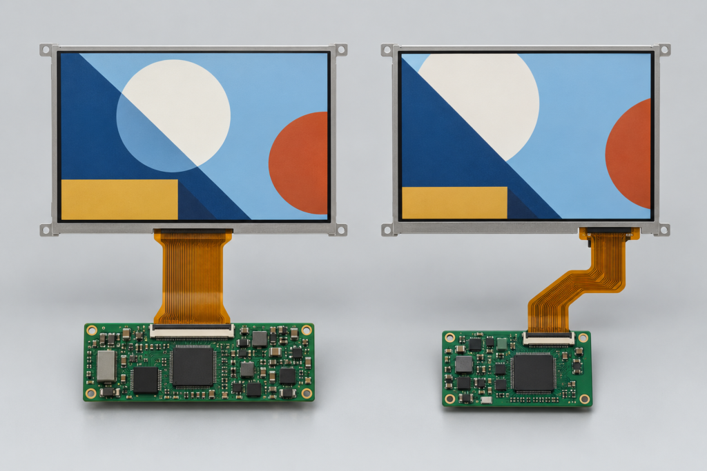
Two modules can use different timing-controller or source-driver designs. Each driver can have its own accepted blanking range, polarity, sampling edge and initialization sequence. A replacement panel may therefore need a new controller-board configuration even when the active pixels match.
Gate-driver integration, source-driver arrangement and internal timing generation can change the required input mode. An integrated timing controller can accept a different range from a module that depends more directly on external timing.
A host may generate a common 60 Hz mode, but the panel datasheet can specify another typical rate or a limited allowable range. Changing the blanking while retaining 60 Hz also changes the required Pixel Clock.
One RGB panel may use SYNC-DE mode while another uses DE-only mode. The FPC can carry similar data lines, yet the controller and pin definition still need different treatment.
Even identical display timing does not prove full compatibility. Check the connector and pin definition, power rails, reset sequence, backlight circuit, touch interface, image orientation, driver support and mechanical fit. Timing is one system layer, not a substitute for the rest of the review.
Parallel RGB makes timing easy to observe. Separate conductors commonly carry red, green and blue data together with Pixel Clock, DE and synchronization signals. The display controller produces the raster timing directly.
This visibility does not make the interface universal. Data width, color ordering, voltage, polarity, sampling edge and timing must still match.
An LVDS transmitter serializes pixel and control information into differential pairs. The panel receiver reconstructs the data. The system still needs a valid native mode, correct LVDS mapping, suitable channel count, supported bit depth and correct clock relationship.
Pixel Clock is related to the transported pixel rate, but it is not the same value as the serial bit rate on an LVDS pair. Serialization ratio and link architecture affect the physical data rate.
MIPI DSI video mode transports a video stream in packets over one or more high-speed data lanes. Active video and blanking requirements affect the data that must cross the link. Lane count, pixel format, operating mode, overhead and D-PHY settings determine whether the host has enough capacity.
The familiar RGB timing values can still appear in the host configuration, but the DSI lane clock is not simply equal to Pixel Clock. Use the SoC, bridge and panel documentation to calculate and validate the link.
Command-mode panels can receive updates through display commands and may use internal frame memory. Their transfer behavior differs from a continuous parallel RGB stream. Do not apply a video-mode calculation without confirming how the selected panel and host implement command mode.
eDP carries standardized packetized display data, while HDMI often appears as an input to a controller board rather than as the native interface of a bare LCD module. A board must still output a panel-supported mode on the internal display side.
An HDMI source showing the correct resolution does not prove that an HDMI-to-MIPI or HDMI-to-LVDS board can drive a given panel. The active conversion depends on the bridge, output interface, panel timing, firmware and physical connection.
Larger blanking intervals increase the horizontal or vertical total. At the same refresh rate, this raises Pixel Clock. More pixel periods per second also increase the rate at which the display pipeline must move data.
The impact extends beyond the panel connector:
A simple framebuffer bandwidth estimate often starts with active pixels, bytes per pixel and frames per second. Real system demand can be higher because of graphics layers, memory bursts, alignment, scaling and other access. Link bandwidth calculations also include encoding or packet overhead that is specific to the interface.
Do not treat one Pixel Clock formula as a complete system bandwidth model. Use it to establish the raster rate, then check each controller, bridge, memory and physical-link limit.
| 症状 | Timing-related checks | Other checks |
|---|---|---|
| Black screen | Pixel Clock, DE, sync mode, polarity | Power, reset, initialization, data path, backlight |
| White screen with backlight | Valid active video and timing | Panel initialization, pinout, interface and controller support |
| Horizontal image shift | HFP, HBP, HSYNC and active width | Data mapping and cropping settings |
| Vertical image shift | VFP, VBP, VSYNC and active height | Rotation, scaling and framebuffer configuration |
| Cropped edge | Active area and total timing | Scaling, OSD or source-mode configuration |
| Repeated or wrapped region | Line or frame boundary values | Framebuffer stride and bridge configuration |
| Flicker | Clock stability, refresh rate, sync and DE | Power noise, backlight PWM, cable and signal integrity |
| Intermittent startup | Timing enable and clock startup | Power sequence, reset, firmware and temperature |
These symptoms are clues, not proof. For example, flicker can come from an unstable Pixel Clock, but it can also come from the LED driver or a poor connector. Diagnose the display as a system.
Record the LCD model and revision, driver IC when available, controller-board model, bridge IC, connector and PCB revision. Compatibility cannot be confirmed from screen size and resolution alone.
Create a table for active resolution, total resolution, porches, sync widths, refresh rate, Pixel Clock, polarity and sampling edge. Compare it with the modes that the controller or firmware can generate.
For LVDS, include mapping, channel count and bit depth. For MIPI DSI, include lane count, pixel format, video or command mode, lane-rate limits and initialization commands. For RGB, include data width and voltage.
A processor may calculate its display clock from a parent clock and integer or fractional divider. The exact requested value may not be available. Confirm the actual generated clock and ensure that the resulting frame rate remains inside the panel limits.
The board support package, device tree, bootloader or controller firmware must describe the correct mode. A hardware-capable board can still fail if the software loads a default timing for another panel.
Correct video timing cannot repair a wrong supply, reset pulse, initialization sequence or LED-driver mismatch. Keep these checks in the same validation plan, but do not confuse them with raster timing.
Test cold power-up, warm restart, signal reconnect, sleep, wake and controlled power-down. Observe whether the clock and active video start only after the panel is ready and whether the backlight exposes an invalid frame.
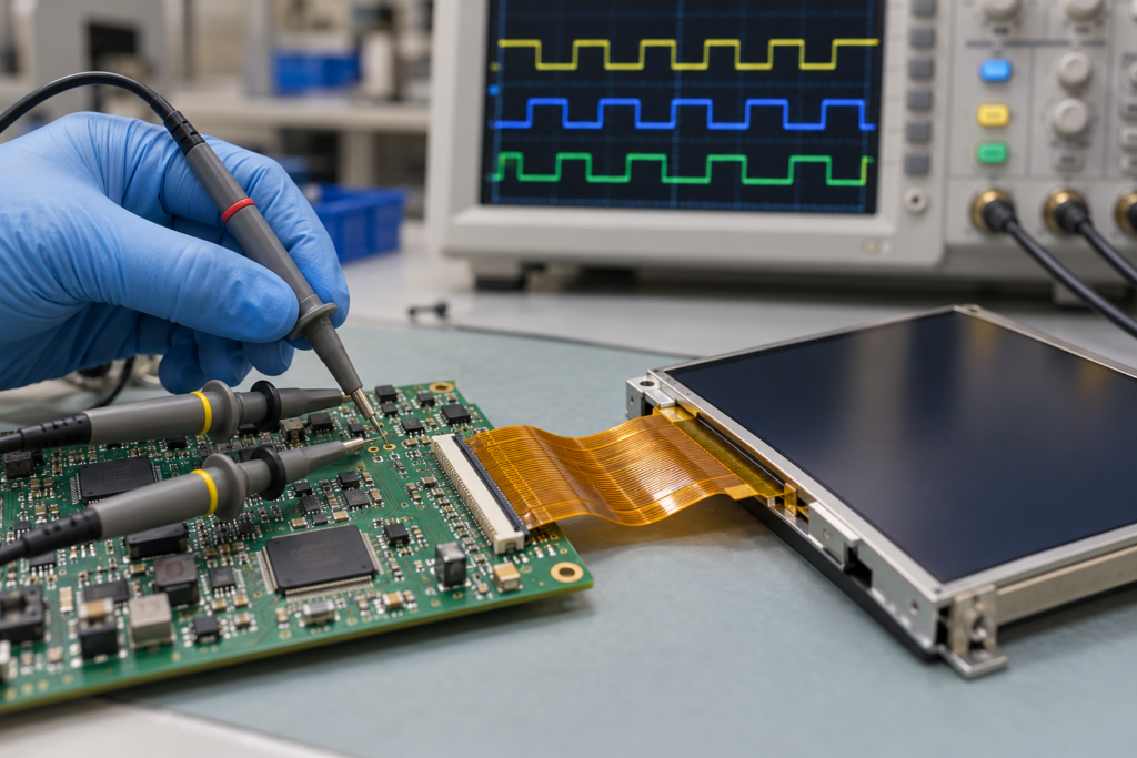
On accessible parallel signals, an oscilloscope can measure Pixel Clock frequency, HSYNC rate, VSYNC rate, DE width, polarity and startup order. From the measured HSYNC and VSYNC rates, engineers can check whether the actual line and frame cadence agrees with the intended mode.
Use probes and bandwidth appropriate for the signal. Poor probing can distort an edge or add enough loading to change behavior. Differential high-speed links require suitable differential measurement equipment and methods.
A logic analyzer can help with lower-speed control signals, GPIO sequencing, SPI initialization or I²C configuration. It is not automatically suitable for capturing every MIPI, LVDS or eDP physical-layer signal. Use protocol-specific equipment when the link speed and signaling method require it.
A measurement shows what the board generates, not what the panel accepts. Compare it with the approved specification.
A typical embedded display configuration can include:
Linux display drivers and device trees often store mode parameters as separate clock, active-area, margin, sync-length and polarity values. An Android-based board can use the same kernel-level configuration concepts even though the user interface runs on Android.
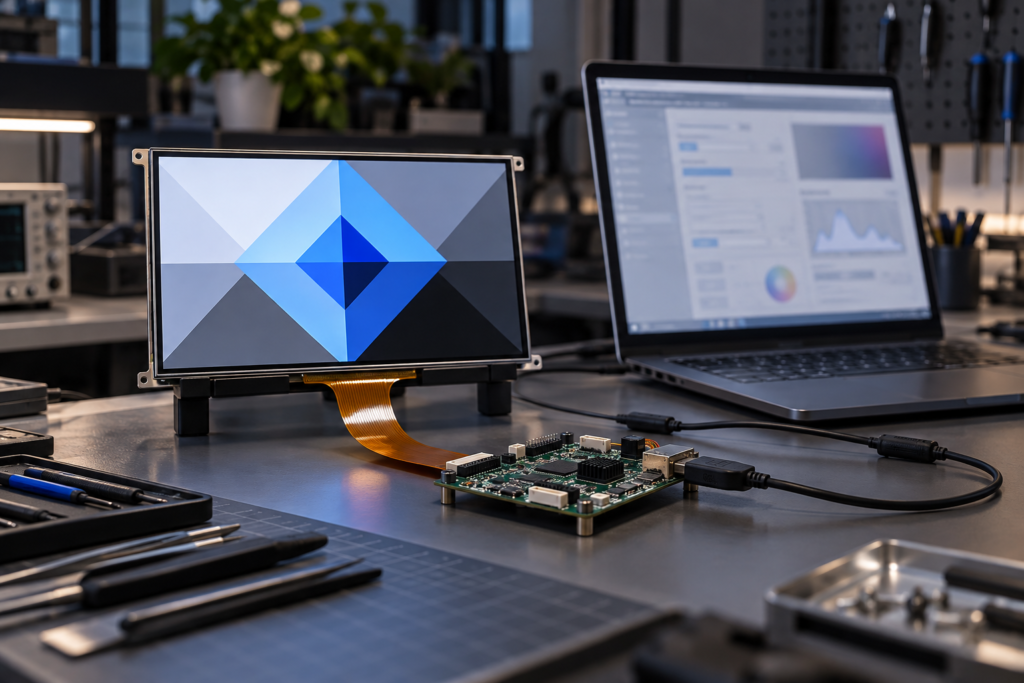
Firmware adaptation is therefore a real part of panel matching. It should be planned with the hardware review rather than treated as a final software setting after the board is complete.
RJY Display can review display timing as part of a project-specific LCD and controller-board configuration. Depending on the selected panel and host platform, the scope can include:
This is a compatibility process, not a universal board claim. The result depends on the exact LCD, controller hardware, firmware, operating system and application environment. An active HDMI-to-MIPI or HDMI-to-LVDS path must be designed for the selected panel; it is not a passive cable conversion.
Send the following information where available:
If the current system already works with another panel, include that panel’s datasheet and approved configuration. A side-by-side comparison often shows whether the difference lies in timing, pinout, interface mode, power or software.
LCD pixel clock connects resolution, blanking and refresh rate, but it is not the only compatibility parameter. Engineers must also preserve the required porches, sync widths, Data Enable behavior, polarity and sampling edge. The chosen interface and firmware then need to carry or generate that mode correctly.
This is why two same-resolution panels can produce different results on the same board. Treat the panel timing table as part of the hardware specification, not as an optional software detail.
For related engineering guidance, review LCD display interfaces, compare MIPI and LVDS for industrial LCDs, を学ぶか、 LVDS data-mapping guide. If you are matching a panel to a host platform, see how to match a TFT LCD with an Android board. For a project review, submit your LCD timing and controller-board information.
Pixel Clock is the rate at which pixel periods advance in a display timing stream. It includes active pixels and the pixel periods used by horizontal and vertical blanking.
Add the active width, horizontal porches and HSYNC width to obtain the horizontal total. Add the active height, vertical porches and VSYNC width to obtain the vertical total. Multiply both totals by the refresh rate. Then compare the result with the panel’s specified clock range.
No. Refresh rate is the number of complete frames per second. Pixel Clock is the number of pixel periods per second. The totals for each line and frame connect the two values.
They can use different driver ICs, blanking intervals, synchronization modes, clock ranges, signal polarities and initialization requirements. Resolution describes only the active pixel matrix.
Do not assume so. A panel can require specific front porch, sync width and back porch ranges even when the total is unchanged. Use the exact datasheet limits and validate the complete system.
The panel may fail to recognize line or frame boundaries. Possible results include a black screen, image shift, unstable display or intermittent operation. These symptoms can also have other causes.
Yes. These interfaces transport display data differently from parallel RGB, but the host, bridge and panel still need a supported native mode. Link mapping, lane configuration, throughput and firmware must also match.
No. A review also needs the LCD model, interface, pin definition, timing, driver IC when available, power, backlight, touch, firmware, operating system and application requirements.
ディスプレイサイズ、解像度、インターフェース、輝度、タッチ要件、コントローラーボード要件、およびアプリケーション環境を共有してください。.
関連するディスプレイ技術ガイドとアプリケーションリファレンスを引き続きお読みください。.
RJYのエンジニアリングチームにご相談いただき、ディスプレイマッチング、コントローラーボードの確認、およびカスタマイズについて話し合ってください。.